- Digital Electronics - Home
- Digital Electronics Basics
- Types of Digital Systems
- Types of Signals
- Logic Levels And Pulse Waveforms
- Digital System Components
- Digital Logic Operations
- Digital Systems Advantages
- Number Systems
- Number Systems
- Binary Numbers Representation
- Binary Arithmetic
- Signed Binary Arithmetic
- Octal Arithmetic
- Hexadecimal Arithmetic
- Complement Arithmetic
- Base Conversions
- Base Conversions
- Binary to Decimal Conversion
- Decimal to Binary Conversion
- Binary to Octal Conversion
- Octal to Binary Conversion
- Octal to Decimal Conversion
- Decimal to Octal Conversion
- Hexadecimal to Binary Conversion
- Binary to Hexadecimal Conversion
- Hexadecimal to Decimal Conversion
- Decimal to Hexadecimal Conversion
- Octal to Hexadecimal Conversion
- Hexadecimal to Octal Conversion
- Binary Codes
- Binary Codes
- 8421 BCD Code
- Excess-3 Code
- Gray Code
- ASCII Codes
- EBCDIC Code
- Code Conversion
- Error Detection & Correction Codes
- Logic Gates
- Logic Gates
- AND Gate
- OR Gate
- NOT Gate
- Universal Gates
- XOR Gate
- XNOR Gate
- CMOS Logic Gate
- OR Gate Using Diode Resistor Logic
- AND Gate vs OR Gate
- Two Level Logic Realization
- Threshold Logic
- Boolean Algebra
- Boolean Algebra
- Laws of Boolean Algebra
- Boolean Functions
- DeMorgan's Theorem
- SOP and POS Form
- POS to Standard POS Form
- Minimization Techniques
- K-Map Minimization
- Three Variable K-Map
- Four Variable K-Map
- Five Variable K-Map
- Six Variable K-Map
- Don't Care Condition
- Quine-McCluskey Method
- Min Terms and Max Terms
- Canonical and Standard Form
- Max Term Representation
- Simplification using Boolean Algebra
- Combinational Logic Circuits
- Digital Combinational Circuits
- Digital Arithmetic Circuits
- Multiplexers
- Multiplexer Design Procedure
- Mux Universal Gate
- 2-Variable Function Using 4:1 Mux
- 3-Variable Function Using 8:1 Mux
- Demultiplexers
- Mux vs Demux
- Parity Bit Generator and Checker
- Comparators
- Encoders
- Keyboard Encoders
- Priority Encoders
- Decoders
- Arithmetic Logic Unit
- 7-Segment LED Display
- Code Converters
- Code Converters
- Binary to Decimal Converter
- Decimal to BCD Converter
- BCD to Decimal Converter
- Binary to Gray Code Converter
- Gray Code to Binary Converter
- BCD to Excess-3 Converter
- Excess-3 to BCD Converter
- Adders
- Half Adders
- Full Adders
- Serial Adders
- Parallel Adders
- Full Adder using Half Adder
- Half Adder vs Full Adder
- Full Adder with NAND Gates
- Half Adder with NAND Gates
- Binary Adder-Subtractor
- Subtractors
- Half Subtractors
- Full Subtractors
- Parallel Subtractors
- Full Subtractor using 2 Half Subtractors
- Half Subtractor using NAND Gates
- Sequential Logic Circuits
- Digital Sequential Circuits
- Clock Signal and Triggering
- Latches
- Shift Registers
- Shift Register Applications
- Binary Registers
- Bidirectional Shift Register
- Counters
- Binary Counters
- Non-binary Counter
- Design of Synchronous Counter
- Synchronous vs Asynchronous Counter
- Finite State Machines
- Algorithmic State Machines
- Flip Flops
- Flip-Flops
- Conversion of Flip-Flops
- D Flip-Flops
- JK Flip-Flops
- T Flip-Flops
- SR Flip-Flops
- Clocked SR Flip-Flop
- Unclocked SR Flip-Flop
- Clocked JK Flip-Flop
- JK to T Flip-Flop
- SR to JK Flip-Flop
- Triggering Methods:Flip-Flop
- Edge-Triggered Flip-Flop
- Master-Slave JK Flip-Flop
- Race-around Condition
- A/D and D/A Converters
- Analog-to-Digital Converter
- Digital-to-Analog Converter
- DAC and ADC ICs
- Realization of Logic Gates
- NOT Gate from NAND Gate
- OR Gate from NAND Gate
- AND Gate from NAND Gate
- NOR Gate from NAND Gate
- XOR Gate from NAND Gate
- XNOR Gate from NAND Gate
- NOT Gate from NOR Gate
- OR Gate from NOR Gate
- AND Gate from NOR Gate
- NAND Gate from NOR Gate
- XOR Gate from NOR Gate
- XNOR Gate from NOR Gate
- NAND/NOR Gate using CMOS
- Full Subtractor using NAND Gate
- AND Gate Using 2:1 MUX
- OR Gate Using 2:1 MUX
- NOT Gate Using 2:1 MUX
- Memory Devices
- Memory Devices
- RAM and ROM
- Cache Memory Design
- Programmable Logic Devices
- Programmable Logic Devices
- Programmable Logic Array
- Programmable Array Logic
- Field Programmable Gate Arrays
- Digital Electronics Families
- Digital Electronics Families
- CPU Architecture
- CPU Architecture
Digital Electronics - Combinational Circuits
A combinational circuit, also called a combinational logic circuit, is a digital electronic circuit whose output is determined by present inputs only.
The output of a combinational logic circuit does not depend on the history of the circuit operation. In other words, a combinational circuit is a digital logic circuit whose output depends only on the present input values and does not depend on any feedback or previous input or output values.
In this chapter, we will explain the fundamentals of combinational circuits, and its block diagram, types, and applications. So, lets start with the basic definition of combinational circuits.
What is a Combinational Circuit?
A combinational circuit is a type of digital logic circuit whose output depends on the present input values only and does not depend on past input and output values. Therefore, a combinational circuit is considered to not have a memory element in its circuit that stores previous inputs and outputs. Instead, it consists of a certain number of input lines to apply current input values and a certain number of output lines.
The most important characteristic of a combinational circuit is that it does not have any feedback path between input and output. Therefore, the combinational circuits can be categorized as open-loop systems.
Block Diagram of Combinational Circuit
The following figure depicts the block diagram of a combinational logic circuit.
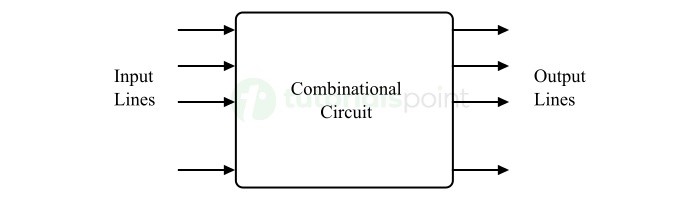
Here, we can see that there are only three key elements in the circuit diagram of a combinational circuit, they are −
- Input Lines − The input lines are used to enter the input values into the combinational circuit.
- Processing Unit − It is the main element that processes the input values depending on the type of the circuit. For example, a full adder adds three binary bits.
- Output Lines − The output lines are used to take results generated by the circuit.
Characteristics of Combinational Circuits
The following are the main characteristics of combinational circuits −
- The output of a combinational circuit, at any instant of time, depends only on the present input values at that instant of time.
- Combinational circuits do not use any kind of memory element in their circuits. Thus, the previous state of input and output values do not have any effect on the present operation of the circuit.
- The output of a combinational circuit can be entirely predicted using its logical operation and input values.
- Combinational circuits produce an instantaneous output in response to any change in its input values.
Types of Combinational Circuits
In digital electronics, the combinational circuits are important components of digital systems. Depending on the functions performed, there are various types of combinational circuits. Some common types of combinational circuits and their functions are explained below −
- Binary Adders
- Binary Subtractors
- Multiplexers (MUX)
- Demultiplexers (DEMUX)
- Encoders
- Decoders
- Comparators
In the following sections of this chapter, we will discuss briefly about each of these combinational circuits along with their functions.
Binary Adders
A binary adder is a combinational circuit that performs the addition of binary digits or bits. Depending on the design and configuration, there are two types of binary adders namely, Half Adder and Full Adder.
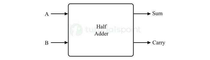
Half Adder
The half adder is a combinational logic circuit with two inputs and two outputs. The half adder circuit is designed to add two single-bit binary numbers A and B. It is the basic building block for the addition of two single-bit numbers. This circuit has two outputs namely, sum and carry.
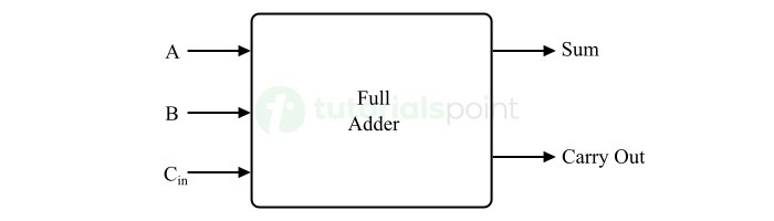
Full Adder
The full adder is designed to overcome the drawback of a half adder which is the ability to add only two bits. Therefore, the full adder is a three-input and two-output combinational circuit. Where, the inputs are two one-bit numbers A and B, and a carry C from the previous addition. The outputs are sum and carry output.
Binary Subtractors
A binary subtractor is a combinational logic circuit used to subtract one binary number from another. Similar to binary adder, there are two types of binary subtractors namely, half-subtractor and full-subtractor.
Half Subtractor
A half subtractor is a combination circuit with two inputs (A and B) and two outputs (difference and borrow). It produces the difference between the two binary bits at the input and also produces an output (Borrow) to indicate if a 1 has been borrowed. In binary subtraction (A-B), A is called a Minuend bit and B is called a Subtrahend bit.

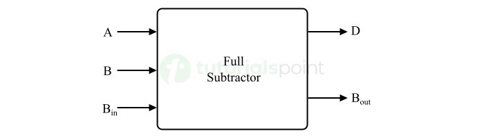
Full Subtractor
The full subtractor is also a combinational circuit with three inputs A, B, and Bin, and two outputs D and Bout.
Here, A is the minuend bit, B is the subtrahend bit, Bin is the previous borrow bit produced by the previous stage, D is the difference output and Bout is the borrow output.
Multiplexers (MUX)
A multiplexer is a special type of combinational logic circuit. It consists of n-data input lines, one output, and m-select lines. For a multiplexer, n = 2m.

A multiplexer is a digital circuit that selects one of the n data inputs and routes it to the output line. The selection of one of the n data inputs is done by the select lines. Depending on the digital code applied at the select lines, one out of "n" data inputs is selected and transmitted to the output line.
In some multiplexers, there is also an enable input E which is useful in cascading of multiple multiplexers.
Depending on the number of input lines, there can be several types of multiplexers. Some common types of multiplexers include 2:1 Multiplexer, 4:1 Multiplexer, 16:1 Multiplexer, and 32:1 Multiplexer.
Demultiplexers (DEMUX)
A demultiplexer performs a distribution operation i.e., it receives one data input and distributes it over several output lines.

A demultiplexer has only one input line, "n" output lines, and "m" select lines. At a time, only one output line is selected by the digital code applied to the select lines and the data input is transmitted to the selected output line.
Demultiplexers can be classified into various types depending on the number of output lines. Some commonly used types of demultiplexers include: 1:2 Demultiplexer, 1:4 Demultiplexer, 1:16 Demultiplexer, and 1:32 Demultiplexer.
Encoders
An encoder is a combinational circuit that is designed to convert a piece of information into a binary code. An encoder has n number of input lines and m number of output lines, where n = 2m.
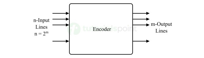
An encoder generates an m-bit binary code corresponding to the digital input applied to it. In other words, an encoder accepts an n-input digital word and converts it into an m-bit another digital word.
Examples of encoder include 4-to-2 encoder, octal-to-binary encoder, hexadecimal-to-binary encoder, priority encoder, etc.
Decoders
A decoder is a combinational circuit that converts a binary code into a normal word like a decimal digit. A decoder typically consists of n input lines and m output lines, where the m = 2n.
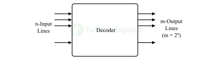
Decoders are widely used in display drivers, data distribution systems, etc.
Some of the commonly used types of decoders are 2 to 4 decoder, 3 to 8 decoder, 4 to 16 decoder, BCD to seven segment decoder, etc.
Comparators
A comparator is a combinational logic circuit developed to compare two binary numbers. Comparators are mainly used in arithmetic and control circuits to perform comparison or logical operations.
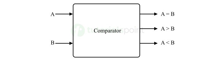
A comparator, as its name suggests, compares the input values and checks whether they are equal or one input is greater/less than the other input.
Limitations of Combinational Circuits
Combinational circuits have several advantages such as fast operational speed, simpler circuit, predictable operation, etc. However, they do have several limitations too, some of which are listed below −
- Combinational circuits do not have any memory element. They are incapable to store history of circuit operation.
- Combinational circuits cannot be used to implement certain highly complex logic functions.
- Combinational circuits do not have any feedback mechanism. That makes the combinational circuits to have limited functionality.
- At large scale, combinational circuits have several design complexities that can result in poor performance and inefficient resource utilization.
Applications of Combinational Circuits
Combinational circuits are the fundamental building blocks in various digital devices and systems. They are widely used in several digital devices in which combinational circuits are used −
- Microprocessors and Microcontrollers
- Digital Computers
- Calculators
- Digital Communication Systems
- Keyboards
- Smartphones and Digital Watches, etc
Conclusion
A combinational logic circuit is a key component in various digital devices and systems. It can be defined as an interconnected system of digital components whose output depends only on the present states of inputs and it does not depend on past input and output values.
In this chapter, we explained the characteristics, limitations, and applications of combinational circuits.