- Digital Electronics - Home
- Digital Electronics Basics
- Types of Digital Systems
- Types of Signals
- Logic Levels And Pulse Waveforms
- Digital System Components
- Digital Logic Operations
- Digital Systems Advantages
- Number Systems
- Number Systems
- Binary Numbers Representation
- Binary Arithmetic
- Signed Binary Arithmetic
- Octal Arithmetic
- Hexadecimal Arithmetic
- Complement Arithmetic
- Base Conversions
- Base Conversions
- Binary to Decimal Conversion
- Decimal to Binary Conversion
- Binary to Octal Conversion
- Octal to Binary Conversion
- Octal to Decimal Conversion
- Decimal to Octal Conversion
- Hexadecimal to Binary Conversion
- Binary to Hexadecimal Conversion
- Hexadecimal to Decimal Conversion
- Decimal to Hexadecimal Conversion
- Octal to Hexadecimal Conversion
- Hexadecimal to Octal Conversion
- Binary Codes
- Binary Codes
- 8421 BCD Code
- Excess-3 Code
- Gray Code
- ASCII Codes
- EBCDIC Code
- Code Conversion
- Error Detection & Correction Codes
- Logic Gates
- Logic Gates
- AND Gate
- OR Gate
- NOT Gate
- Universal Gates
- XOR Gate
- XNOR Gate
- CMOS Logic Gate
- OR Gate Using Diode Resistor Logic
- AND Gate vs OR Gate
- Two Level Logic Realization
- Threshold Logic
- Boolean Algebra
- Boolean Algebra
- Laws of Boolean Algebra
- Boolean Functions
- DeMorgan's Theorem
- SOP and POS Form
- POS to Standard POS Form
- Minimization Techniques
- K-Map Minimization
- Three Variable K-Map
- Four Variable K-Map
- Five Variable K-Map
- Six Variable K-Map
- Don't Care Condition
- Quine-McCluskey Method
- Min Terms and Max Terms
- Canonical and Standard Form
- Max Term Representation
- Simplification using Boolean Algebra
- Combinational Logic Circuits
- Digital Combinational Circuits
- Digital Arithmetic Circuits
- Multiplexers
- Multiplexer Design Procedure
- Mux Universal Gate
- 2-Variable Function Using 4:1 Mux
- 3-Variable Function Using 8:1 Mux
- Demultiplexers
- Mux vs Demux
- Parity Bit Generator and Checker
- Comparators
- Encoders
- Keyboard Encoders
- Priority Encoders
- Decoders
- Arithmetic Logic Unit
- 7-Segment LED Display
- Code Converters
- Code Converters
- Binary to Decimal Converter
- Decimal to BCD Converter
- BCD to Decimal Converter
- Binary to Gray Code Converter
- Gray Code to Binary Converter
- BCD to Excess-3 Converter
- Excess-3 to BCD Converter
- Adders
- Half Adders
- Full Adders
- Serial Adders
- Parallel Adders
- Full Adder using Half Adder
- Half Adder vs Full Adder
- Full Adder with NAND Gates
- Half Adder with NAND Gates
- Binary Adder-Subtractor
- Subtractors
- Half Subtractors
- Full Subtractors
- Parallel Subtractors
- Full Subtractor using 2 Half Subtractors
- Half Subtractor using NAND Gates
- Sequential Logic Circuits
- Digital Sequential Circuits
- Clock Signal and Triggering
- Latches
- Shift Registers
- Shift Register Applications
- Binary Registers
- Bidirectional Shift Register
- Counters
- Binary Counters
- Non-binary Counter
- Design of Synchronous Counter
- Synchronous vs Asynchronous Counter
- Finite State Machines
- Algorithmic State Machines
- Flip Flops
- Flip-Flops
- Conversion of Flip-Flops
- D Flip-Flops
- JK Flip-Flops
- T Flip-Flops
- SR Flip-Flops
- Clocked SR Flip-Flop
- Unclocked SR Flip-Flop
- Clocked JK Flip-Flop
- JK to T Flip-Flop
- SR to JK Flip-Flop
- Triggering Methods:Flip-Flop
- Edge-Triggered Flip-Flop
- Master-Slave JK Flip-Flop
- Race-around Condition
- A/D and D/A Converters
- Analog-to-Digital Converter
- Digital-to-Analog Converter
- DAC and ADC ICs
- Realization of Logic Gates
- NOT Gate from NAND Gate
- OR Gate from NAND Gate
- AND Gate from NAND Gate
- NOR Gate from NAND Gate
- XOR Gate from NAND Gate
- XNOR Gate from NAND Gate
- NOT Gate from NOR Gate
- OR Gate from NOR Gate
- AND Gate from NOR Gate
- NAND Gate from NOR Gate
- XOR Gate from NOR Gate
- XNOR Gate from NOR Gate
- NAND/NOR Gate using CMOS
- Full Subtractor using NAND Gate
- AND Gate Using 2:1 MUX
- OR Gate Using 2:1 MUX
- NOT Gate Using 2:1 MUX
- Memory Devices
- Memory Devices
- RAM and ROM
- Cache Memory Design
- Programmable Logic Devices
- Programmable Logic Devices
- Programmable Logic Array
- Programmable Array Logic
- Field Programmable Gate Arrays
- Digital Electronics Families
- Digital Electronics Families
- CPU Architecture
- CPU Architecture
Asynchronous or Unclocked SR Flip-Flop
What is SR Flip-Flop?
In digital electronics, the SR flip-flop is a sequential logic circuit that have two inputs, i.e. S and R, and two outputs, i.e. Q and Q'.
The input S represent "Set" and the input R represents "Reset". The output Q is the normal output of the flip-flop, and Q' is the inverted output of the flip-flop, it is the complement of the normal output Q of the flip-flop. The SR flip flop is a one-bit storage device used in several digital electronics systems.
The basic block diagram of an SR flip-flop is shown in Figure-1.

Based on the presence or absence of clock signal, SR flip-flop can be classified into two types namely, synchronous SR flip-flop and asynchronous SR flip-flop. The synchronous SR flip-flop is one which generates output only when clock signal is activated. Hence, it is also known as clocked SR flip-flop.
On the other hand, an asynchronous SR flip-flop is one whose output is available at any time the inputs are applied to the circuit. Asynchronous SR flip flop is also known as unclocked SR flip-flop because its output is not controlled by the clock signal, but only controlled by inputs applied.
As the title of this article implies, here we shall only talk about asynchronous or unclocked SR flip flop.
What is Asynchronous SR Flip Flop?
An asynchronous SR flip flop, also called unclocked SR flip-flop or simply SR latch, is a sequential logic circuit which is used to store one bit binary information. It has two inputs and two outputs. The inputs are S (represents "Set" input) and R (represents "Reset" input) of the flip-flop. The first output is Q which is called normal output of the flip-flop, and another output is Q', which is called complemented output.
The block diagram of an asynchronous or unclocked SR flip-flop is shown in Figure-2.

The unclocked or asynchronous SR flip flop can be constructed by using two cross coupled NOR gates or NAND gates.
Let us now discuss each construction (using NOR gates and using NAND gates) of the SR flip-flop along with their operation and truth table.
Asynchronous SR Flip-Flop using NOR Gates
As mentioned earlier, the unclocked SR flip flop can be constructed by using two cross-coupled NOR gates as shown in Figure-3.
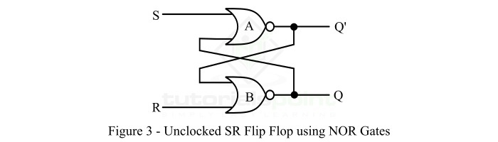
It has two inputs namely S (Set) and R (Reset), and two outputs namely Q (Normal output) and Q' (Inverted output).
This asynchronous SR flip flop for different possible combinations of inputs S and R operates as described as below −
- When S = 0 and R = 0 − In this case, the inputs to both NOR gates are logic 0. Hence, there is no effect on the output of the circuit. As a result, the outputs remain in their previous states. This condition of the unclocked SR flip flop is called "No Change" or "Hold Condition".
- When S = 1 and R = 0 − In this case, the output of the NOR gate A will become zero because the input S is logic 1. As a result, both inputs of the NOR gate B become logic 0, and thus, the output of the NOR gate B is logic 1 making Q equal to 1. This is called "set condition" of the unclocked SR flip flop.
- When S = 0 and R = 1 − In this case, the output of the NOR gate B will become zero because the input R is logic 1, i.e. Q = 0. As a result, both inputs of the NOR gate A become logic 0, and thus, the output of the NOR gate A is logic 1 making Q' equal to 1 and Q = 0. This is called "reset condition" of the unclocked SR flip-flop.
- When S = 1 and R = 1 − This is called "forbidden condition or invalid state" of the SR flip-flop, because this combination of inputs forces the output of both NOR gates to become logic 0, which is not possible.
Truth Table of SR Flip Flop
The truth table of unclocked SR flip flop based on the above described operation is given below.
| S | R | Q | Description |
|---|---|---|---|
| 0 | 0 | NC | No Change |
| 0 | 1 | 0 | Reset |
| 1 | 0 | 1 | Set |
| 1 | 1 | X | Forbidden |
Asynchronous SR Flip-Flop using NAND Gates
We can also implement the unclocked SR flip-flop by using two cross coupled NAND gates. The asynchronous SR flip flop using NAND gates is shown in Figure-4 below.
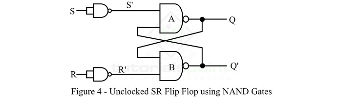
It can be seen that the asynchronous SR flip flop is an active low input SR flip flop. Now, let us discuss the working of the asynchronous SR flip flop for different possible input combinations.
- When S = 0 and R = 0, i.e. S' = 1 and R' = 1 − In this case both inputs i.e. S' and R' are Logic 1, thus the output remains in previous state. This is called hold state of the SR flip flop.
- When S = 0 and R = 1, i.e. S' = 1 and R' = 0 − In this case, the input S' is Logic 1 and input R' is Logic 0. Thus, the output of the NAND gate B will become logic 1. Therefore, the output of the NAND gate A, i.e. Q becomes logic 1. This is called reset state of the flip flop.
- When S = 1 and R = 0, i.e. S' = 0 and R' = 1 − In this case, the input S' is logic 0 and input R' is logic 1. As the input S' is logic 0, thus the output of the NAND gate A, i.e. Q becomes logic 1. This is called set state of the SR flip flop.
- When S = 1 and R = 1, i.e. S' = 0 and R' = 0 − In this case, both inputs are logic 0, i.e., outputs of both NAND gates must be logic 1 which is not allowed because the outputs must be complement of each other. This is called forbidden or invalid state of the flip flop.
Truth Table of Asynchronous SR Flip Flop using NAND Gates
Based on this discussion, we can derive the truth table of the asynchronous SR flip flop realized using NAND gates.
| S | S' | R | R' | Q | Description |
|---|---|---|---|---|---|
| 0 | 1 | 0 | 1 | NC | No Change |
| 0 | 1 | 1 | 0 | 0 | Reset |
| 1 | 0 | 0 | 1 | 1 | Set |
| 1 | 0 | 1 | 0 | X | Forbidden |
This is all about Asynchronous or Unclocked SR Flip Flop in digital electronics.