- VLSI Design Tutorial
- VLSI Design - Home
- VLSI Design - Digital System
- VLSI Design - FPGA Technology
- VLSI Design - MOS Transistor
- VLSI Design - MOS Inverter
- Combinational MOS Logic Circuits
- Sequential MOS Logic Circuits
- VHDL Programming
- VHDL - Introduction
- VHDL - Combinational Circuits
- VHDL - Sequential Circuits
- VLSI Design Useful Resources
- VLSI Design - Quick Guide
- VLSI Design - Useful Resources
- VLSI Design - Discussion
VLSI Design - FPGA Technology
FPGA – Introduction
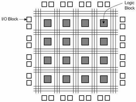
The full form of FPGA is “Field Programmable Gate Array”. It contains ten thousand to more than a million logic gates with programmable interconnection. Programmable interconnections are available for users or designers to perform given functions easily. A typical model FPGA chip is shown in the given figure. There are I/O blocks, which are designed and numbered according to function. For each module of logic level composition, there are CLB’s (Configurable Logic Blocks).
CLB performs the logic operation given to the module. The inter connection between CLB and I/O blocks are made with the help of horizontal routing channels, vertical routing channels and PSM (Programmable Multiplexers).
The number of CLB it contains only decides the complexity of FPGA. The functionality of CLB’s and PSM are designed by VHDL or any other hardware descriptive language. After programming, CLB and PSM are placed on chip and connected with each other with routing channels.
Advantages
- It requires very small time; starting from design process to functional chip.
- No physical manufacturing steps are involved in it.
- The only disadvantage is, it is costly than other styles.
Gate Array Design
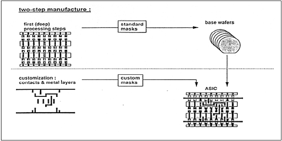
The gate array (GA) ranks second after the FPGA, in terms of fast prototyping capability. While user programming is important to the design implementation of the FPGA chip, metal mask design and processing is used for GA. Gate array implementation requires a two-step manufacturing process.
The first phase results in an array of uncommitted transistors on each GA chip. These uncommitted chips can be stored for later customization, which is completed by defining the metal interconnects between the transistors of the array. The patterning of metallic interconnects is done at the end of the chip fabrication process, so that the turn-around time can still be short, a few days to a few weeks. The figure given below shows the basic processing steps for gate array implementation.
Typical gate array platforms use dedicated areas called channels, for inter-cell routing between rows or columns of MOS transistors. They simplify the interconnections. Interconnection patterns that perform basic logic gates are stored in a library, which can then be used to customize rows of uncommitted transistors according to the netlist.
In most of the modern GAs, multiple metal layers are used for channel routing. With the use of multiple interconnected layers, the routing can be achieved over the active cell areas; so that the routing channels can be removed as in Sea-of-Gates (SOG) chips. Here, the entire chip surface is covered with uncommitted nMOS and pMOS transistors. The neighboring transistors can be customized using a metal mask to form basic logic gates.
For inter cell routing, some of the uncommitted transistors must be sacrificed. This design style results in more flexibility for interconnections and usually in a higher density. GA chip utilization factor is measured by the used chip area divided by the total chip area. It is higher than that of the FPGA and so is the chip speed.
Standard Cell Based Design
A standard cell based design requires development of a full custom mask set. The standard cell is also known as the polycell. In this approach, all of the commonly used logic cells are developed, characterized and stored in a standard cell library.
A library may contain a few hundred cells including inverters, NAND gates, NOR gates, complex AOI, OAI gates, D-latches and Flip-flops. Each gate type can be implemented in several versions to provide adequate driving capability for different fan-outs. The inverter gate can have standard size, double size, and quadruple size so that the chip designer can select the proper size to obtain high circuit speed and layout density.
Each cell is characterized according to several different characterization categories, such as,
- Delay time versus load capacitance
- Circuit simulation model
- Timing simulation model
- Fault simulation model
- Cell data for place-and-route
- Mask data
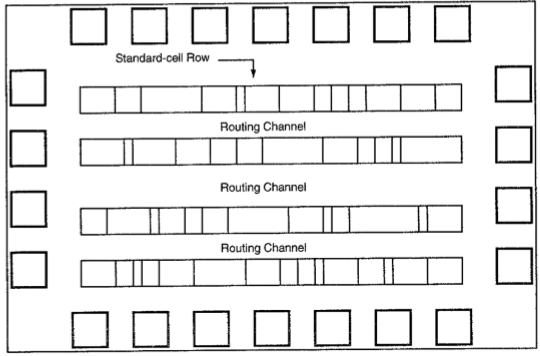
For automated placement of the cells and routing, each cell layout is designed with a fixed height, so that a number of cells can be bounded side-by-side to form rows. The power and ground rails run parallel to the upper and lower boundaries of the cell. So that, neighboring cells share a common power bus and a common ground bus. The figure shown below is a floorplan for standard-cell based design.
Full Custom Design
In a full-custom design, the entire mask design is made new, without the use of any library. The development cost of this design style is rising. Thus, the concept of design reuse is becoming famous to reduce design cycle time and development cost.
The hardest full custom design can be the design of a memory cell, be it static or dynamic. For logic chip design, a good negotiation can be obtained using a combination of different design styles on the same chip, i.e. standard cells, data-path cells, and programmable logic arrays (PLAs).
Practically, the designer does the full custom layout, i.e. the geometry, orientation, and placement of every transistor. The design productivity is usually very low; typically a few tens of transistors per day, per designer. In digital CMOS VLSI, full-custom design is hardly used due to the high labor cost. These design styles include the design of high-volume products such as memory chips, high-performance microprocessors and FPGA.