- Network Theory Tutorial
- Network Theory - Home
- Network Theory - Overview
- Example Problems
- Network Theory - Active Elements
- Network Theory - Passive Elements
- Network Theory - Kirchhoff’s Laws
- Electrical Quantity Division Principles
- Network Theory - Nodal Analysis
- Network Theory - Mesh Analysis
- Network Theory - Equivalent Circuits
- Equivalent Circuits Example Problem
- Delta to Star Conversion
- Star to Delta Conversion
- Network Theory - Network Topology
- Network Topology Matrices
- Superposition Theorem
- Thevenin’s Theorem
- Network Theory - Norton’s Theorem
- Maximum Power Transfer Theorem
- Response of DC Circuits
- Response of AC Circuits
- Network Theory - Series Resonance
- Parallel Resonance
- Network Theory - Coupled Circuits
- Two-Port Networks
- Two-Port Parameter Conversions
- Network Theory - Filters
- Network Theory Useful Resources
- Network Theory - Quick Guide
- Network Theory - Useful Resources
- Network Theory - Discussion
Network Theory - Quick Guide
Network Theory - Overview
Network theory is the study of solving the problems of electric circuits or electric networks. In this introductory chapter, let us first discuss the basic terminology of electric circuits and the types of network elements.
Basic Terminology
In Network Theory, we will frequently come across the following terms −
- Electric Circuit
- Electric Network
- Current
- Voltage
- Power
So, it is imperative that we gather some basic knowledge on these terms before proceeding further. Let’s start with Electric Circuit.
Electric Circuit
An electric circuit contains a closed path for providing a flow of electrons from a voltage source or current source. The elements present in an electric circuit will be in series connection, parallel connection, or in any combination of series and parallel connections.
Electric Network
An electric network need not contain a closed path for providing a flow of electrons from a voltage source or current source. Hence, we can conclude that "all electric circuits are electric networks" but the converse need not be true.
Current
The current "I" flowing through a conductor is nothing but the time rate of flow of charge. Mathematically, it can be written as
$$I = \frac{dQ}{dt}$$
Where,
Q is the charge and its unit is Coloumb.
t is the time and its unit is second.
As an analogy, electric current can be thought of as the flow of water through a pipe. Current is measured in terms of Ampere.
In general, Electron current flows from negative terminal of source to positive terminal, whereas, Conventional current flows from positive terminal of source to negative terminal.
Electron current is obtained due to the movement of free electrons, whereas, Conventional current is obtained due to the movement of free positive charges. Both of these are called as electric current.
Voltage
The voltage "V" is nothing but an electromotive force that causes the charge (electrons) to flow. Mathematically, it can be written as
$$V = \frac{dW}{dQ}$$
Where,
W is the potential energy and its unit is Joule.
Q is the charge and its unit is Coloumb.
As an analogy, Voltage can be thought of as the pressure of water that causes the water to flow through a pipe. It is measured in terms of Volt.
Power
The power "P" is nothing but the time rate of flow of electrical energy. Mathematically, it can be written as
$$P = \frac{dW}{dt}$$
Where,
W is the electrical energy and it is measured in terms of Joule.
t is the time and it is measured in seconds.
We can re-write the above equation a
$$P = \frac{dW}{dt} = \frac{dW}{dQ} \times \frac{dQ}{dt} = VI$$
Therefore, power is nothing but the product of voltage V and current I. Its unit is Watt.
Types of Network Elements
We can classify the Network elements into various types based on some parameters. Following are the types of Network elements −
Active Elements and Passive Elements
Linear Elements and Non-linear Elements
Bilateral Elements and Unilateral Elements
Active Elements and Passive Elements
We can classify the Network elements into either active or passive based on the ability of delivering power.
Active Elements deliver power to other elements, which are present in an electric circuit. Sometimes, they may absorb the power like passive elements. That means active elements have the capability of both delivering and absorbing power. Examples: Voltage sources and current sources.
Passive Elements can’t deliver power (energy) to other elements, however they can absorb power. That means these elements either dissipate power in the form of heat or store energy in the form of either magnetic field or electric field. Examples: Resistors, Inductors, and capacitors.
Linear Elements and Non-Linear Elements
We can classify the network elements as linear or non-linear based on their characteristic to obey the property of linearity.
Linear Elements are the elements that show a linear relationship between voltage and current. Examples: Resistors, Inductors, and capacitors.
Non-Linear Elements are those that do not show a linear relation between voltage and current. Examples: Voltage sources and current sources.
Bilateral Elements and Unilateral Elements
Network elements can also be classified as either bilateral or unilateral based on the direction of current flows through the network elements.
Bilateral Elements are the elements that allow the current in both directions and offer the same impedance in either direction of current flow. Examples: Resistors, Inductors and capacitors.
The concept of Bilateral elements is illustrated in the following figures.
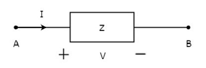
In the above figure, the current (I) is flowing from terminals A to B through a passive element having impedance of Z Ω. It is the ratio of voltage (V) across that element between terminals A & B and current (I).
In the above figure, the current (I) is flowing from terminals B to A through a passive element having impedance of Z Ω. That means the current (–I) is flowing from terminals A to B. In this case too, we will get the same impedance value, since both the current and voltage having negative signs with respect to terminals A & B.
Unilateral Elements are those that allow the current in only one direction. Hence, they offer different impedances in both directions.
Network Theory - Example Problems
We discussed the types of network elements in the previous chapter. Now, let us identify the nature of network elements from the V-I characteristics given in the following examples.
Example 1
The V-I characteristics of a network element is shown below.
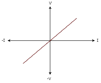
Step 1 − Verifying the network element as linear or non-linear.
From the above figure, the V-I characteristics of a network element is a straight line passing through the origin. Hence, it is a Linear element.
Step 2 − Verifying the network element as active or passive.
The given V-I characteristics of a network element lies in the first and third quadrants.
In the first quadrant, the values of both voltage (V) and current (I) are positive. So, the ratios of voltage (V) and current (I) gives positive impedance values.
Similarly, in the third quadrant, the values of both voltage (V) and current (I) have negative values. So, the ratios of voltage (V) and current (I) produce positive impedance values.
Since, the given V-I characteristics offer positive impedance values, the network element is a Passive element.
Step 3 − Verifying the network element as bilateral or unilateral.
For every point (I, V) on the characteristics, there exists a corresponding point (-I, -V) on the given characteristics. Hence, the network element is a Bilateral element.
Therefore, the given V-I characteristics show that the network element is a Linear, Passive, and Bilateral element.
Example 2
The V-I characteristics of a network element is shown below.
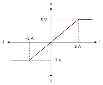
Step 1 − Verifying the network element as linear or non-linear.
From the above figure, the V-I characteristics of a network element is a straight line only between the points (-3A, -3V) and (5A, 5V). Beyond these points, the V-I characteristics are not following the linear relation. Hence, it is a Non-linear element.
Step 2 − Verifying the network element as active or passive.
The given V-I characteristics of a network element lies in the first and third quadrants. In these two quadrants, the ratios of voltage (V) and current (I) produce positive impedance values. Hence, the network element is a Passive element.
Step 3 − Verifying the network element as bilateral or unilateral.
Consider the point (5A, 5V) on the characteristics. The corresponding point (-5A, -3V) exists on the given characteristics instead of (-5A, -5V). Hence, the network element is a Unilateral element.
Therefore, the given V-I characteristics show that the network element is a Non-linear, Passive, and Unilateral element.
Network Theory - Active Elements
Active Elements are the network elements that deliver power to other elements present in an electric circuit. So, active elements are also called as sources of voltage or current type. We can classify these sources into the following two categories −
- Independent Sources
- Dependent Sources
Independent Sources
As the name suggests, independent sources produce fixed values of voltage or current and these are not dependent on any other parameter. Independent sources can be further divided into the following two categories −
- Independent Voltage Sources
- Independent Current Sources
Independent Voltage Sources
An independent voltage source produces a constant voltage across its two terminals. This voltage is independent of the amount of current that is flowing through the two terminals of voltage source.
Independent ideal voltage source and its V-I characteristics are shown in the following figure.
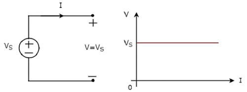
The V-I characteristics of an independent ideal voltage source is a constant line, which is always equal to the source voltage (VS) irrespective of the current value (I). So, the internal resistance of an independent ideal voltage source is zero Ohms.
Hence, the independent ideal voltage sources do not exist practically, because there will be some internal resistance.
Independent practical voltage source and its V-I characteristics are shown in the following figure.
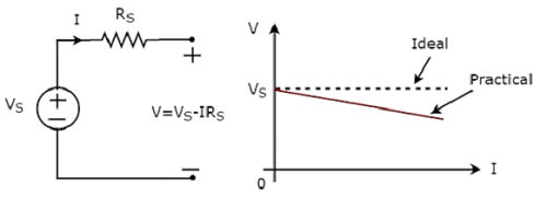
There is a deviation in the V-I characteristics of an independent practical voltage source from the V-I characteristics of an independent ideal voltage source. This is due to the voltage drop across the internal resistance (RS) of an independent practical voltage source.
Independent Current Sources
An independent current source produces a constant current. This current is independent of the voltage across its two terminals. Independent ideal current source and its V-I characteristics are shown in the following figure.
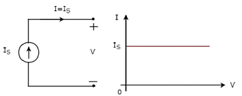
The V-I characteristics of an independent ideal current source is a constant line, which is always equal to the source current (IS) irrespective of the voltage value (V). So, the internal resistance of an independent ideal current source is infinite ohms.
Hence, the independent ideal current sources do not exist practically, because there will be some internal resistance.
Independent practical current source and its V-I characteristics are shown in the following figure.
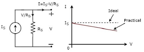
There is a deviation in the V-I characteristics of an independent practical current source from the V-I characteristics of an independent ideal current source. This is due to the amount of current flows through the internal shunt resistance (RS) of an independent practical current source.
Dependent Sources
As the name suggests, dependent sources produce the amount of voltage or current that is dependent on some other voltage or current. Dependent sources are also called as controlled sources. Dependent sources can be further divided into the following two categories −
- Dependent Voltage Sources
- Dependent Current Sources
Dependent Voltage Sources
A dependent voltage source produces a voltage across its two terminals. The amount of this voltage is dependent on some other voltage or current. Hence, dependent voltage sources can be further classified into the following two categories −
- Voltage Dependent Voltage Source (VDVS)
- Current Dependent Voltage Source (CDVS)
Dependent voltage sources are represented with the signs ‘+’ and ‘-’ inside a diamond shape. The magnitude of the voltage source can be represented outside the diamond shape.
Dependent Current Sources
A dependent current source produces a current. The amount of this current is dependent on some other voltage or current. Hence, dependent current sources can be further classified into the following two categories −
- Voltage Dependent Current Source (VDCS)
- Current Dependent Current Source (CDCS)
Dependent current sources are represented with an arrow inside a diamond shape. The magnitude of the current source can be represented outside the diamond shape.
We can observe these dependent or controlled sources in equivalent models of transistors.
Source Transformation Technique
We know that there are two practical sources, namely, voltage source and current source. We can transform (convert) one source into the other based on the requirement, while solving network problems.
The technique of transforming one source into the other is called as source transformation technique. Following are the two possible source transformations −
- Practical voltage source into a practical current source
- Practical current source into a practical voltage source
Practical voltage source into a practical current source
The transformation of practical voltage source into a practical current source is shown in the following figure
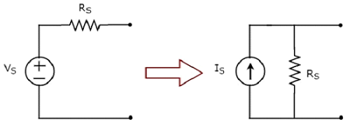
Practical voltage source consists of a voltage source (VS) in series with a resistor (RS). This can be converted into a practical current source as shown in the figure. It consists of a current source (IS) in parallel with a resistor (RS).
The value of IS will be equal to the ratio of VS and RS. Mathematically, it can be represented as
$$I_S = \frac{V_S}{R_S}$$
Practical current source into a practical voltage source
The transformation of practical current source into a practical voltage source is shown in the following figure.
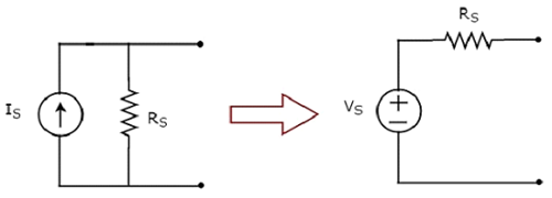
Practical current source consists of a current source (IS) in parallel with a resistor (RS). This can be converted into a practical voltage source as shown in the figure. It consists of a voltage source (VS) in series with a resistor (RS).
The value of VS will be equal to the product of IS and RS. Mathematically, it can be represented as
$$V_S = I_S R_S$$
Network Theory - Passive Elements
In this chapter, we will discuss in detail about the passive elements such as Resistor, Inductor, and Capacitor. Let us start with Resistors.
Resistor
The main functionality of Resistor is either opposes or restricts the flow of electric current. Hence, the resistors are used in order to limit the amount of current flow and / or dividing (sharing) voltage.
Let the current flowing through the resistor is I amperes and the voltage across it is V volts. The symbol of resistor along with current, I and voltage, V are shown in the following figure.
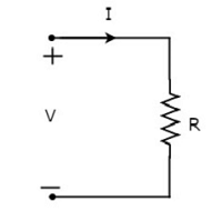
According to Ohm’s law, the voltage across resistor is the product of current flowing through it and the resistance of that resistor. Mathematically, it can be represented as
$V = IR$ Equation 1
$\Rightarrow I = \frac{V}{R}$Equation 2
Where, R is the resistance of a resistor.
From Equation 2, we can conclude that the current flowing through the resistor is directly proportional to the applied voltage across resistor and inversely proportional to the resistance of resistor.
Power in an electric circuit element can be represented as
$P = VI$Equation 3
Substitute, Equation 1 in Equation 3.
$P = (IR)I$
$\Rightarrow P = I^2 R$ Equation 4
Substitute, Equation 2 in Equation 3.
$P = V \lgroup \frac{V}{R} \rgroup$
$\Rightarrow P = \frac{V^2}{R}$ Equation 5
So, we can calculate the amount of power dissipated in the resistor by using one of the formulae mentioned in Equations 3 to 5.
Inductor
In general, inductors will have number of turns. Hence, they produce magnetic flux when current flows through it. So, the amount of total magnetic flux produced by an inductor depends on the current, I flowing through it and they have linear relationship.
Mathematically, it can be written as
$$\Psi \: \alpha \: I$$
$$\Rightarrow \Psi = LI$$
Where,
Ψ is the total magnetic flux
L is the inductance of an inductor
Let the current flowing through the inductor is I amperes and the voltage across it is V volts. The symbol of inductor along with current I and voltage V are shown in the following figure.
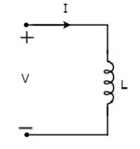
According to Faraday’s law, the voltage across the inductor can be written as
$$V = \frac{d\Psi}{dt}$$
Substitute Ψ = LI in the above equation.
$$V = \frac{d(LI)}{dt}$$
$$\Rightarrow V = L \frac{dI}{dt}$$
$$\Rightarrow I = \frac{1}{L} \int V dt$$
From the above equations, we can conclude that there exists a linear relationship between voltage across inductor and current flowing through it.
We know that power in an electric circuit element can be represented as
$$P = VI$$
Substitute $V = L \frac{dI}{dt}$ in the above equation.
$$P = \lgroup L \frac{dI}{dt}\rgroup I$$
$$\Rightarrow P = LI \frac{dI}{dt}$$
By integrating the above equation, we will get the energy stored in an inductor as
$$W = \frac{1}{2} LI^2$$
So, the inductor stores the energy in the form of magnetic field.
Capacitor
In general, a capacitor has two conducting plates, separated by a dielectric medium. If positive voltage is applied across the capacitor, then it stores positive charge. Similarly, if negative voltage is applied across the capacitor, then it stores negative charge.
So, the amount of charge stored in the capacitor depends on the applied voltage V across it and they have linear relationship. Mathematically, it can be written as
$$Q \: \alpha \: V$$
$$\Rightarrow Q = CV$$
Where,
Q is the charge stored in the capacitor.
C is the capacitance of a capacitor.
Let the current flowing through the capacitor is I amperes and the voltage across it is V volts. The symbol of capacitor along with current I and voltage V are shown in the following figure.
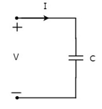
We know that the current is nothing but the time rate of flow of charge. Mathematically, it can be represented as
$$I = \frac{dQ}{dt}$$
Substitute $Q = CV$ in the above equation.
$$I = \frac{d(CV)}{dt}$$
$$\Rightarrow I = C \frac{dV}{dt}$$
$$\Rightarrow V = \frac{1}{C} \int I dt$$
From the above equations, we can conclude that there exists a linear relationship between voltage across capacitor and current flowing through it.
We know that power in an electric circuit element can be represented as
$$P = VI$$
Substitute $I = C \frac{dV}{dt}$ in the above equation.
$$P = V \lgroup C \frac{dV}{dt} \rgroup$$
$$\Rightarrow P = CV \frac{dV}{dt}$$
By integrating the above equation, we will get the energy stored in the capacitor as
$$W = \frac{1}{2}CV^2$$
So, the capacitor stores the energy in the form of electric field.
Network Theory - Kirchhoff’s Laws
Network elements can be either of active or passive type. Any electrical circuit or network contains one of these two types of network elements or a combination of both.
Now, let us discuss about the following two laws, which are popularly known as Kirchhoff’s laws.
- Kirchhoff’s Current Law
- Kirchhoff’s Voltage Law
Kirchhoff’s Current Law
Kirchhoff’s Current Law (KCL) states that the algebraic sum of currents leaving (or entering) a node is equal to zero.
A Node is a point where two or more circuit elements are connected to it. If only two circuit elements are connected to a node, then it is said to be simple node. If three or more circuit elements are connected to a node, then it is said to be Principal Node.
Mathematically, KCL can be represented as
$$\displaystyle\sum\limits_{m=1}^M I_m = 0$$
Where,
Im is the mth branch current leaving the node.
M is the number of branches that are connected to a node.
The above statement of KCL can also be expressed as "the algebraic sum of currents entering a node is equal to the algebraic sum of currents leaving a node". Let us verify this statement through the following example.
Example
Write KCL equation at node P of the following figure.
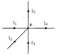
In the above figure, the branch currents I1, I2 and I3 are entering at node P. So, consider negative signs for these three currents.
In the above figure, the branch currents I4 and I5 are leaving from node P. So, consider positive signs for these two currents.
The KCL equation at node P will be
$$- I_1 - I_2 - I_3 + I_4 + I_5 = 0$$
$$\Rightarrow I_1 + I_2 + I_3 = I_4 + I_5$$
In the above equation, the left-hand side represents the sum of entering currents, whereas the right-hand side represents the sum of leaving currents.
In this tutorial, we will consider positive sign when the current leaves a node and negative sign when it enters a node. Similarly, you can consider negative sign when the current leaves a node and positive sign when it enters a node. In both cases, the result will be same.
Note − KCL is independent of the nature of network elements that are connected to a node.
Kirchhoff’s Voltage Law
Kirchhoff’s Voltage Law (KVL) states that the algebraic sum of voltages around a loop or mesh is equal to zero.
A Loop is a path that terminates at the same node where it started from. In contrast, a Mesh is a loop that doesn’t contain any other loops inside it.
Mathematically, KVL can be represented as
$$\displaystyle\sum\limits_{n=1}^N V_n = 0$$
Where,
Vn is the nth element’s voltage in a loop (mesh).
N is the number of network elements in the loop (mesh).
The above statement of KVL can also be expressed as "the algebraic sum of voltage sources is equal to the algebraic sum of voltage drops that are present in a loop." Let us verify this statement with the help of the following example.
Example
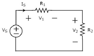
Write KVL equation around the loop of the following circuit.
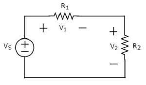
The above circuit diagram consists of a voltage source, VS in series with two resistors R1 and R2. The voltage drops across the resistors R1 and R2 are V1 and V2 respectively.
Apply KVL around the loop.
$$V_S - V_1 - V_2 = 0$$
$$\Rightarrow V_S = V_1 + V_2$$
In the above equation, the left-hand side term represents single voltage source VS. Whereas, the right-hand side represents the sum of voltage drops. In this example, we considered only one voltage source. That’s why the left-hand side contains only one term. If we consider multiple voltage sources, then the left side contains sum of voltage sources.
In this tutorial, we consider the sign of each element’s voltage as the polarity of the second terminal that is present while travelling around the loop. Similarly, you can consider the sign of each voltage as the polarity of the first terminal that is present while travelling around the loop. In both cases, the result will be same.
Note − KVL is independent of the nature of network elements that are present in a loop.
Electrical Quantity Division Principles
In this chapter, let us discuss about the following two division principles of electrical quantities.
- Current Division Principle
- Voltage Division Principle
Current Division Principle
When two or more passive elements are connected in parallel, the amount of current that flows through each element gets divided (shared) among themselves from the current that is entering the node.
Consider the following circuit diagram.
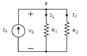
The above circuit diagram consists of an input current source IS in parallel with two resistors R1 and R2. The voltage across each element is VS. The currents flowing through the resistors R1 and R2 are I1 and I2 respectively.
The KCL equation at node P will be
$$I_S = I_1 + I_2$$
Substitute $I_1 = \frac{V_S}{R_1}$ and $I_2 = \frac{V_S}{R_2}$ in the above equation.
$$I_S = \frac{V_S}{R_1} + \frac{V_S}{R_2} = V_S \lgroup \frac {R_2 + R_1 }{R_1 R_2} \rgroup$$
$$\Rightarrow V_S = I_S \lgroup \frac{R_1R_2}{R_1 + R_2} \rgroup$$
Substitute the value of VS in $I_1 = \frac{V_S}{R_1}$.
$$I_1 = \frac{I_S}{R_1}\lgroup \frac{R_1 R_2}{R_1 + R_2} \rgroup$$
$$\Rightarrow I_1 = I_S\lgroup \frac{R_2}{R_1 + R_2} \rgroup$$
Substitute the value of VS in $I_2 = \frac{V_S}{R_2}$.
$$I_2 = \frac{I_S}{R_2} \lgroup \frac{R_1 R_2}{R_1 + R_2} \rgroup$$
$$\Rightarrow I_2 = I_S \lgroup \frac{R_1}{R_1 + R_2} \rgroup$$
From equations of I1 and I2, we can generalize that the current flowing through any passive element can be found by using the following formula.
$$I_N = I_S \lgroup \frac{Z_1\rVert Z_2 \rVert...\rVert Z_{N-1}}{Z_1 + Z_2 + ... + Z_N}\rgroup$$
This is known as current division principle and it is applicable, when two or more passive elements are connected in parallel and only one current enters the node.
Where,
IN is the current flowing through the passive element of Nth branch.
IS is the input current, which enters the node.
Z1, Z2, …,ZN are the impedances of 1st branch, 2nd branch, …, Nth branch respectively.
Voltage Division Principle
When two or more passive elements are connected in series, the amount of voltage present across each element gets divided (shared) among themselves from the voltage that is available across that entire combination.
Consider the following circuit diagram.
The above circuit diagram consists of a voltage source, VS in series with two resistors R1 and R2. The current flowing through these elements is IS. The voltage drops across the resistors R1 and R2 are V1 and V2 respectively.
The KVL equation around the loop will be
$$V_S = V_1 + V_2$$
Substitute V1 = IS R1 and V2 = IS R2 in the above equation
$$V_S = I_S R_1 + I_S R_2 = I_S(R_1 + R_2)$$
$$I_S = \frac{V_S}{R_1 + R_2}$$
Substitute the value of IS in V1 = IS R1.
$$V_1 = \lgroup \frac {V_S}{R_1 + R_2} \rgroup R_1$$
$$\Rightarrow V_1 = V_S \lgroup \frac {R_1}{R_1 + R_2} \rgroup$$
Substitute the value of IS in V2 = IS R2.
$$V_2 = \lgroup \frac {V_S}{R_1 + R_2} \rgroup R_2$$
$$\Rightarrow V_2 = V_S \lgroup \frac {R_2}{R_1 + R_2} \rgroup$$
From equations of V1 and V2, we can generalize that the voltage across any passive element can be found by using the following formula.
$$V_N = V_S \lgroup \frac {Z_N}{Z_1 + Z_2 +....+ Z_N}\rgroup$$
This is known as voltage division principle and it is applicable, when two or more passive elements are connected in series and only one voltage available across the entire combination.
Where,
VN is the voltage across Nth passive element.
VS is the input voltage, which is present across the entire combination of series passive elements.
Z1,Z2, …,Z3 are the impedances of 1st passive element, 2nd passive element, …, Nth passive element respectively.
Network Theory - Nodal Analysis
There are two basic methods that are used for solving any electrical network: Nodal analysis and Mesh analysis. In this chapter, let us discuss about the Nodal analysis method.
In Nodal analysis, we will consider the node voltages with respect to Ground. Hence, Nodal analysis is also called as Node-voltage method.
Procedure of Nodal Analysis
Follow these steps while solving any electrical network or circuit using Nodal analysis.
Step 1 − Identify the principal nodes and choose one of them as reference node. We will treat that reference node as the Ground.
Step 2 − Label the node voltages with respect to Ground from all the principal nodes except the reference node.
Step 3 − Write nodal equations at all the principal nodes except the reference node. Nodal equation is obtained by applying KCL first and then Ohm’s law.
Step 4 − Solve the nodal equations obtained in Step 3 in order to get the node voltages.
Now, we can find the current flowing through any element and the voltage across any element that is present in the given network by using node voltages.
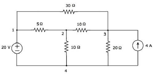
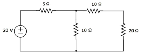
Example
Find the current flowing through 20 Ω resistor of the following circuit using Nodal analysis.
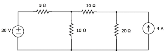
Step 1 − There are three principle nodes in the above circuit. Those are labelled as 1, 2, and 3 in the following figure.
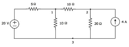
In the above figure, consider node 3 as reference node (Ground).
Step 2 − The node voltages, V1 and V2, are labelled in the following figure.
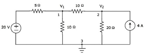
In the above figure, V1 is the voltage from node 1 with respect to ground and V2 is the voltage from node 2 with respect to ground.
Step 3 − In this case, we will get two nodal equations, since there are two principal nodes, 1 and 2, other than Ground. When we write the nodal equations at a node, assume all the currents are leaving from the node for which the direction of current is not mentioned and that node’s voltage as greater than other node voltages in the circuit.
The nodal equation at node 1 is
$$\frac{V_1 - 20}{5} + \frac{V_1}{10} + \frac{V_1 - V_2}{10} = 0$$
$$\Rightarrow \frac{2 V_1 - 40 + V_1 + V_1 - V_2}{10} = 0$$
$$\Rightarrow 4V_1 - 40 - V_2 = 0$$
$\Rightarrow V_2 = 4V_1 - 40$ Equation 1
The nodal equation at node 2 is
$$-4 + \frac{V_2}{20} + \frac{V_2 - V_1}{10} = 0$$
$$\Rightarrow \frac{-80 + V_2 + 2V_2 - 2V_2}{20} = 0$$
$\Rightarrow 3V_2 − 2V_1 = 80$ Equation 2
Step 4 − Finding node voltages, V1 and V2 by solving Equation 1 and Equation 2.
Substitute Equation 1 in Equation 2.
$$3(4 V_1 - 40) - 2 V_1 = 80$$
$$\Rightarrow 12 V_1 - 120 - 2V_1 =80$$
$$\Rightarrow 10 V_1 = 200$$
$$\Rightarrow V_1 = 20V$$
Substitute V1 = 20 V in Equation1.
$$V_2 = 4(20) - 40$$
$$\Rightarrow V_2 = 40V$$
So, we got the node voltages V1 and V2 as 20 V and 40 V respectively.
Step 5 − The voltage across 20 Ω resistor is nothing but the node voltage V2 and it is equal to 40 V. Now, we can find the current flowing through 20 Ω resistor by using Ohm’s law.
$$I_{20 \Omega} = \frac{V_2}{R}$$
Substitute the values of V2 and R in the above equation.
$$I_{20 \Omega} = \frac{40}{20}$$
$$\Rightarrow I_{20 \Omega} = 2A$$
Therefore, the current flowing through 20 Ω resistor of given circuit is 2 A.
Note − From the above example, we can conclude that we have to solve ‘n’ nodal equations, if the electric circuit has ‘n’ principal nodes (except the reference node). Therefore, we can choose Nodal analysis when the number of principal nodes (except reference node) is less than the number of meshes of any electrical circuit.
Network Theory - Mesh Analysis
In Mesh analysis, we will consider the currents flowing through each mesh. Hence, Mesh analysis is also called as Mesh-current method.
A branch is a path that joins two nodes and it contains a circuit element. If a branch belongs to only one mesh, then the branch current will be equal to mesh current.
If a branch is common to two meshes, then the branch current will be equal to the sum (or difference) of two mesh currents, when they are in same (or opposite) direction.
Procedure of Mesh Analysis
Follow these steps while solving any electrical network or circuit using Mesh analysis.
Step 1 − Identify the meshes and label the mesh currents in either clockwise or anti-clockwise direction.
Step 2 − Observe the amount of current that flows through each element in terms of mesh currents.
Step 3 − Write mesh equations to all meshes. Mesh equation is obtained by applying KVL first and then Ohm’s law.
Step 4 − Solve the mesh equations obtained in Step 3 in order to get the mesh currents.
Now, we can find the current flowing through any element and the voltage across any element that is present in the given network by using mesh currents.
Example
Find the voltage across 30 Ω resistor using Mesh analysis.
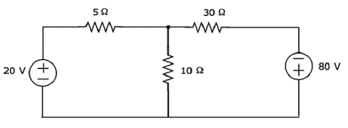
Step 1 − There are two meshes in the above circuit. The mesh currents I1 and I2 are considered in clockwise direction. These mesh currents are shown in the following figure.
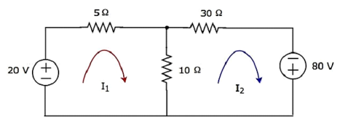
Step 2 − The mesh current I1 flows through 20 V voltage source and 5 Ω resistor. Similarly, the mesh current I2 flows through 30 Ω resistor and -80 V voltage source. But, the difference of two mesh currents, I1 and I2, flows through 10 Ω resistor, since it is the common branch of two meshes.
Step 3 − In this case, we will get two mesh equations since there are two meshes in the given circuit. When we write the mesh equations, assume the mesh current of that particular mesh as greater than all other mesh currents of the circuit.
The mesh equation of first mesh is
$$20 - 5I_1 -10(I_1 - I_2) = 0$$
$$\Rightarrow 20 - 15I_1 + 10I_2 = 0$$
$$\Rightarrow 10I_2 = 15I_1 - 20$$
Divide the above equation with 5.
$$2I_2 = 3I_1 - 4$$
Multiply the above equation with 2.
$4I_2 = 6I_1 - 8$ Equation 1
The mesh equation of second mesh is
$$-10(I_2 - I_1) - 30I_2 + 80 = 0$$
Divide the above equation with 10.
$$-(I_2 - I_1) - 3I_2 + 8 = 0$$
$$\Rightarrow -4I_2 + I_1 + 8 = 0$$
$4I_2 = I_1 + 8$ Equation 2
Step 4 − Finding mesh currents I1 and I2 by solving Equation 1 and Equation 2.
The left-hand side terms of Equation 1 and Equation 2 are the same. Hence, equate the right-hand side terms of Equation 1 and Equation 2 in order find the value of I1.
$$6I_1 - 8 = I_1 + 8$$
$$\Rightarrow 5I_1 = 16$$
$$\Rightarrow I_1 = \frac{16}{5} A$$
Substitute I1 value in Equation 2.
$$4I_2 = \frac{16}{5} + 8$$
$$\Rightarrow 4I_2 = \frac{56}{5}$$
$$\Rightarrow I_2 = \frac{14}{5} A$$
So, we got the mesh currents I1 and I2 as $\mathbf{\frac{16}{5}}$ A and $\mathbf{\frac{14}{5}}$ A respectively.
Step 5 − The current flowing through 30 Ω resistor is nothing but the mesh current I2 and it is equal to $\frac{14}{5}$ A. Now, we can find the voltage across 30 Ω resistor by using Ohm’s law.
$$V_{30 \Omega} = I_2 R$$
Substitute the values of I2 and R in the above equation.
$$V_{30 \Omega} = \lgroup \frac{14}{5} \rgroup 30$$
$$\Rightarrow V_{30 \Omega} = 84V$$
Therefore, the voltage across 30 Ω resistor of the given circuit is 84 V.
Note 1 − From the above example, we can conclude that we have to solve ‘m’ mesh equations, if the electric circuit is having ‘m’ meshes. That’s why we can choose Mesh analysis when the number of meshes is less than the number of principal nodes (except the reference node) of any electrical circuit.
Note 2 − We can choose either Nodal analysis or Mesh analysis, when the number of meshes is equal to the number of principal nodes (except the reference node) in any electric circuit.
Network Theory - Equivalent Circuits
If a circuit consists of two or more similar passive elements and are connected in exclusively of series type or parallel type, then we can replace them with a single equivalent passive element. Hence, this circuit is called as an equivalent circuit.
In this chapter, let us discuss about the following two equivalent circuits.
- Series Equivalent Circuit
- Parallel Equivalent Circuit
Series Equivalent Circuit
If similar passive elements are connected in series, then the same current will flow through all these elements. But, the voltage gets divided across each element.
Consider the following circuit diagram.
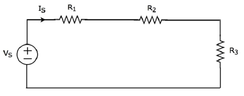
It has a single voltage source (VS) and three resistors having resistances of R1, R2 and R3. All these elements are connected in series. The current IS flows through all these elements.
The above circuit has only one mesh. The KVL equation around this mesh is
$$V_S = V_1 + V_2 + V_3$$
Substitute $V_1 = I_S R_1, \: V_2 = I_S R_2$ and $V_3 = I_S R_3$ in the above equation.
$$V_S = I_S R_1 + I_S R_2 + I_S R_3$$
$$\Rightarrow V_S = I_S(R_1 + R_2 + R_3)$$
The above equation is in the form of $V_S = I_S R_{Eq}$ where,
$$R_{Eq} = R_1 + R_2 + R_3$$
The equivalent circuit diagram of the given circuit is shown in the following figure.
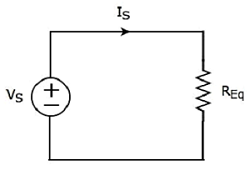
That means, if multiple resistors are connected in series, then we can replace them with an equivalent resistor. The resistance of this equivalent resistor is equal to sum of the resistances of all those multiple resistors.
Note 1 − If ‘N’ inductors having inductances of L1, L2, ..., LN are connected in series, then the equivalent inductance will be
$$L_{Eq} = L_1 + L_2 + ... + L_N$$
Note 2 − If ‘N’ capacitors having capacitances of C1, C2, ..., CN are connected in series, then the equivalent capacitance will be
$$\frac{1}{C_{Eq}} = \frac{1}{C_1} + \frac{1}{C_2} + ... + \frac{1}{C_N}$$
Parallel Equivalent Circuit
If similar passive elements are connected in parallel, then the same voltage will be maintained across each element. But, the current flowing through each element gets divided.
Consider the following circuit diagram.
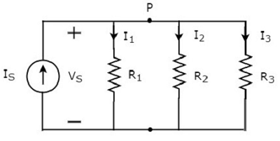
It has a single current source (IS) and three resistors having resistances of R1, R2, and R3. All these elements are connected in parallel. The voltage (VS) is available across all these elements.
The above circuit has only one principal node (P) except the Ground node. The KCL equation at this principal node (P) is
$$I_S = I_1 + I_2 + I_3$$
Substitute $I_1 = \frac{V_S}{R_1}, \: I_2 = \frac{V_S}{R_2}$ and $I_3 = \frac{V_S}{R_3}$ in the above equation.
$$I_S = \frac{V_S}{R_1} + \frac{V_S}{R_2} + \frac{V_S}{R_3}$$
$$\Rightarrow I_S = V_S \lgroup \frac{1}{R_1} + \frac{1}{R_2} + \frac{1}{R_3} \rgroup$$
$$\Rightarrow V_S = I_S\left [ \frac{1}{\lgroup \frac{1}{R_1} + \frac{1}{R_2} + \frac{1}{R_3} \rgroup} \right ]$$
The above equation is in the form of VS = ISREq where,
$$R_{Eq} = \frac{1}{\lgroup \frac{1}{R_1} + \frac{1}{R_2} + \frac{1}{R_3} \rgroup}$$
$$\frac{1}{R_{Eq}} = \frac{1}{R_1} + \frac{1}{R_2} + \frac{1}{R_3}$$
The equivalent circuit diagram of the given circuit is shown in the following figure.
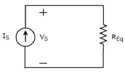
That means, if multiple resistors are connected in parallel, then we can replace them with an equivalent resistor. The resistance of this equivalent resistor is equal to the reciprocal of sum of reciprocal of each resistance of all those multiple resistors.
Note 1 − If ‘N’ inductors having inductances of L1, L2, ..., LN are connected in parallel, then the equivalent inductance will be
$$\frac{1}{L_{Eq}} = \frac{1}{L_1} + \frac{1}{L_2} + ... + \frac{1}{L_N}$$
Note 2 − If ‘N’ capacitors having capacitances of C1, C2, ..., CN are connected in parallel, then the equivalent capacitance will be
$$C_{Eq} = C_1 + C_2 + ... + C_N$$
Equivalent Circuits Example Problem
In the previous chapter, we discussed about the equivalent circuits of series combination and parallel combination individually. In this chapter, let us solve an example problem by considering both series and parallel combinations of similar passive elements.
Example
Let us find the equivalent resistance across the terminals A & B of the following electrical network.
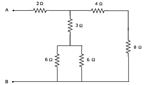
We will get the equivalent resistance across terminals A & B by minimizing the above network into a single resistor between those two terminals. For this, we have to identify the combination of resistors that are connected in series form and parallel form and then find the equivalent resistance of the respective form in every step.
The given electrical network is modified into the following form as shown in the following figure.
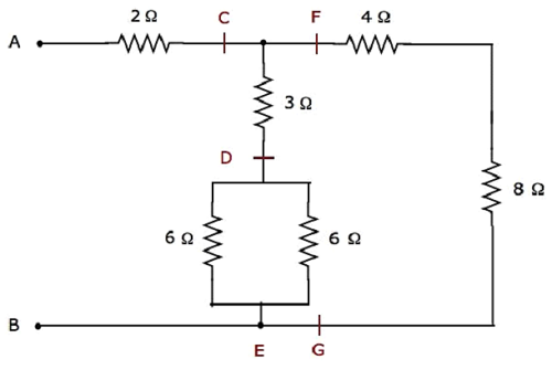
In the above figure, the letters, C to G, are used for labelling various terminals.
Step 1 − In the above network, two 6 Ω resistors are connected in parallel. So, the equivalent resistance between D & E will be 3 Ω. This can be obtained by doing the following simplification.
$$R_{DE} = \frac{6 \times 6}{6 + 6} = \frac{36}{12} = 3 \Omega$$
In the above network, the resistors 4 Ω and 8 Ω are connected in series. So, the equivalent resistance between F & G will be 12 Ω. This can be obtained by doing the following simplification.
$$R_{FG} = 4 + 8 = 12 \Omega$$
Step 2 − The simplified electrical network after Step 1 is shown in the following figure.
In the above network, two 3 Ω resistors are connected in series. So, the equivalent resistance between C & E will be 6 Ω. This can be obtained by doing the following simplification.
$$R_{CE} = 3 + 3 = 6 \Omega$$
Step 3 − The simplified electrical network after Step 2 is shown in the following figure.
In the above network, the resistors 6 Ω and 12 Ω are connected in parallel. So, the equivalent resistance between C & B will be 4 Ω. This can be obtained by doing the following simplification.
$$R_{CB} = \frac{6 \times 12}{6 + 12} = \frac{72}{18} = 4 \Omega$$
Step 4 − The simplified electrical network after Step 3 is shown in the following figure.
In the above network, the resistors 2 Ω and 4 Ω are connected in series between the terminals A & B. So, the equivalent resistance between A & B will be 6 Ω. This can be obtained by doing the following simplification.
$$R_{AB} = 2 + 4 = 6 \Omega$$
Therefore, the equivalent resistance between terminals A & B of the given electrical network is 6 Ω.
Network Theory - Delta to Star Conversion
In the previous chapter, we discussed an example problem related equivalent resistance. There, we calculated the equivalent resistance between the terminals A & B of the given electrical network easily. Because, in every step, we got the combination of resistors that are connected in either series form or parallel form.
However, in some situations, it is difficult to simplify the network by following the previous approach. For example, the resistors connected in either delta (δ) form or star form. In such situations, we have to convert the network of one form to the other in order to simplify it further by using series combination or parallel combination. In this chapter, let us discuss about the Delta to Star Conversion.
Delta Network
Consider the following delta network as shown in the following figure.
The following equations represent the equivalent resistance between two terminals of delta network, when the third terminal is kept open.
$$R_{AB} = \frac{(R_1 + R_3)R_2}{R_1 + R_2 + R_3}$$
$$R_{BC} = \frac{(R_1 + R_2)R_3}{R_1 + R_2 + R_3}$$
$$R_{CA} = \frac{(R_2 + R_3)R_1}{R_1 + R_2 + R_3}$$
Star Network
The following figure shows the equivalent star network corresponding to the above delta network.
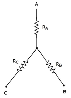
The following equations represent the equivalent resistance between two terminals of star network, when the third terminal is kept open.
$$R_{AB} = R_A + R_B$$
$$R_{BC} = R_B + R_C$$
$$R_{CA} = R_C + R_A$$
Star Network Resistances in terms of Delta Network Resistances
We will get the following equations by equating the right-hand side terms of the above equations for which the left-hand side terms are same.
$R_A + R_B = \frac{(R_1 + R_3)R_2}{R_1 + R_2 + R_3}$ Equation 1
$R_B + R_C = \frac{(R_1 + R_2)R_3}{R_1 + R_2 + R_3}$ Equation 2
$R_C + R_A = \frac{(R_2 + R_3)R_1}{R_1 + R_2 + R_3}$ Equation 3
By adding the above three equations, we will get
$$2(R_A + R_B + R_C) = \frac{2(R_1 R_2 + R_2 R_3 + R_3 R_1)}{R_1 + R_2 + R_3}$$
$\Rightarrow R_A + R_B + R_C = \frac{R_1 R_2 + R_2 R_3 + R_3 R_1}{R_1 + R_2 + R_3}$ Equation 4
Subtract Equation 2 from Equation 4.
$R_A + R_B + R_C - (R_B + R_C) = \frac{R_1 R_2 + R_2 R_3 + R_3 R_1}{R_1 + R_2 + R_3} - \frac{(R_1 + R_2)R_3}{R_1 + R_2 + R_3}$
$$R_A = \frac{R_1 R_2}{R_1 + R_2 + R_3}$$
By subtracting Equation 3 from Equation 4, we will get
$$R_B = \frac{R_2 R_3}{R_1 + R_2 + R_3}$$
By subtracting Equation 1 from Equation 4, we will get
$$R_C = \frac{R_3 R_1}{R_1 + R_2 + R_3}$$
By using the above relations, we can find the resistances of star network from the resistances of delta network. In this way, we can convert a delta network into a star network.
Example
Let us calculate the resistances of star network, which are equivalent to that of delta network as shown in the following figure.
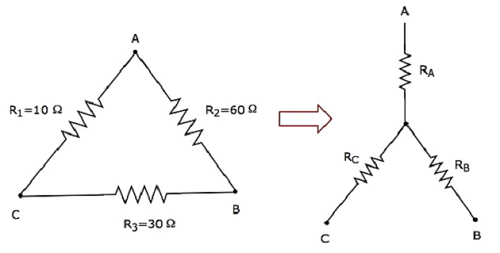
Given the resistances of delta network as R1 = 10 Ω, R2 = 60 Ω and R3 = 30 Ω.
We know the following relations of the resistances of star network in terms of resistances of delta network.
$$R_A = \frac{R_1 R_2}{R_1 + R_2 + R_3}$$
$$R_B = \frac{R_2 R_3}{R_1 + R_2 + R_3}$$
$$R_C = \frac{R_3 R_1}{R_1 + R_2 + R_3}$$
Substitute the values of R1, R2 and R3 in the above equations.
$$R_A = \frac{10 \times 60}{10 +60+30} = \frac{600}{100} = 6\Omega$$
$$R_B = \frac{60 \times 30}{10 +60+30} = \frac{1800}{100} = 18\Omega$$
$$R_C = \frac{30 \times 10}{10 +60+30} = \frac{300}{100} = 3\Omega$$
So, we got the resistances of star network as RA = 6 Ω, RB = 18 Ω and RC = 3 Ω, which are equivalent to the resistances of the given delta network.
Network Theory - Star to Delta Conversion
In the previous chapter, we discussed about the conversion of delta network into an equivalent star network. Now, let us discuss about the conversion of star network into an equivalent delta network. This conversion is called as Star to Delta Conversion.
In the previous chapter, we got the resistances of star network from delta network as
$R_A = \frac{R_1 R_2}{R_1 + R_2 + R_3}$ Equation 1
$R_B = \frac{R_2 R_3}{R_1 + R_2 + R_3}$ Equation 2
$R_C = \frac{R_3 R_1}{R_1 + R_2 + R_3}$ Equation 3
Delta Network Resistances in terms of Star Network Resistances
Let us manipulate the above equations in order to get the resistances of delta network in terms of resistances of star network.
Multiply each set of two equations and then add.
$$R_A R_B + R_B R_C + R_C R_A = \frac{R_1 R_2^2 R_3 + R_2 R_3^2 R_1 + R_3 R_1^2 R_2}{(R_1 + R_2 + R_3)^2}$$
$$\Rightarrow R_A R_B + R_B R_C + R_C R_A = \frac{R_1 R_2 R_3(R_1 + R_2 + R_3)}{(R_1 + R_2 + R_3)^2}$$
$\Rightarrow R_A R_B + R_B R_C + R_C R_A = \frac{R_1 R_2 R_3}{R_1 + R_2 + R_3}$ Equation 4
By dividing Equation 4 with Equation 2, we will get
$$\frac{R_A R_B + R_B R_C + R_C R_A}{R_B} = R_1$$
$$\Rightarrow R_1 = R_C + R_A + \frac{R_C R_A}{R_B}$$
By dividing Equation 4 with Equation 3, we will get
$$R_2 = R_A + R_B + \frac{R_A R_B}{R_C}$$
By dividing Equation 4 with Equation 1, we will get
$$R_3 = R_B + R_C + \frac{R_B R_C}{R_A}$$
By using the above relations, we can find the resistances of delta network from the resistances of star network. In this way, we can convert star network into delta network.
Example
Let us calculate the resistances of delta network, which are equivalent to that of star network as shown in the following figure.
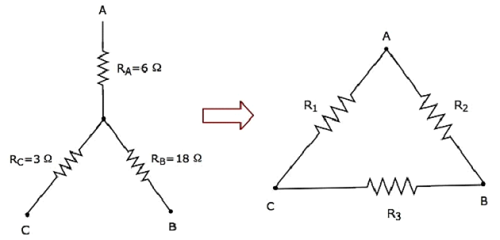
Given the resistances of star network as RA = 6 Ω, RB = 18 Ω and RC = 3 Ω.
We know the following relations of the resistances of delta network in terms of resistances of star network.
$$R_1 = R_C + R_A + \frac{R_C R_A}{R_B}$$
$$R_2 = R_A + R_B + \frac{R_A R_B}{R_C}$$
$$R_3 = R_B + R_C + \frac{R_B R_C}{R_A}$$
Substitute the values of RA, RB and RC in the above equations.
$$R_1 = 3 + 6 + \frac{3 \times 6}{18} = 9 + 1 = 10 \Omega$$
$$R_2 = 6 + 18 + \frac{6 \times 18}{3} = 24 + 36 = 60 \Omega$$
$$R_3 = 18 + 3 + \frac{18 \times 3}{6} = 21 + 9 = 30 \Omega$$
So, we got the resistances of delta network as R1 = 10 Ω, R2 = 60 Ω and R3 = 30 Ω, which are equivalent to the resistances of the given star network.
Network Theory - Network Topology
Network topology is a graphical representation of electric circuits. It is useful for analyzing complex electric circuits by converting them into network graphs. Network topology is also called as Graph theory.
Basic Terminology of Network Topology
Now, let us discuss about the basic terminology involved in this network topology.
Graph
Network graph is simply called as graph. It consists of a set of nodes connected by branches. In graphs, a node is a common point of two or more branches. Sometimes, only a single branch may connect to the node. A branch is a line segment that connects two nodes.
Any electric circuit or network can be converted into its equivalent graph by replacing the passive elements and voltage sources with short circuits and the current sources with open circuits. That means, the line segments in the graph represent the branches corresponding to either passive elements or voltage sources of electric circuit.
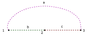
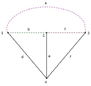
Example
Let us consider the following electric circuit.
In the above circuit, there are four principal nodes and those are labelled with 1, 2, 3, and 4. There are seven branches in the above circuit, among which one branch contains a 20 V voltage source, another branch contains a 4 A current source and the remaining five branches contain resistors having resistances of 30 Ω, 5 Ω, 10 Ω, 10 Ω and 20 Ω respectively.
An equivalent graph corresponding to the above electric circuit is shown in the following figure.
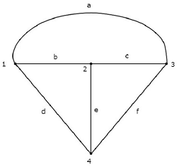
In the above graph, there are four nodes and those are labelled with 1, 2, 3 & 4 respectively. These are same as that of principal nodes in the electric circuit. There are six branches in the above graph and those are labelled with a, b, c, d, e & f respectively.
In this case, we got one branch less in the graph because the 4 A current source is made as open circuit, while converting the electric circuit into its equivalent graph.
From this Example, we can conclude the following points −
The number of nodes present in a graph will be equal to the number of principal nodes present in an electric circuit.
The number of branches present in a graph will be less than or equal to the number of branches present in an electric circuit.
Types of Graphs
Following are the types of graphs −
- Connected Graph
- Unconnected Graph
- Directed Graph
- Undirected Graph
Now, let us discuss these graphs one by one.
Connected Graph
If there exists at least one branch between any of the two nodes of a graph, then it is called as a connected graph. That means, each node in the connected graph will be having one or more branches that are connected to it. So, no node will present as isolated or separated.
The graph shown in the previous Example is a connected graph. Here, all the nodes are connected by three branches.
Unconnected Graph
If there exists at least one node in the graph that remains unconnected by even single branch, then it is called as an unconnected graph. So, there will be one or more isolated nodes in an unconnected graph.
Consider the graph shown in the following figure.
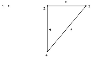
In this graph, the nodes 2, 3, and 4 are connected by two branches each. But, not even a single branch has been connected to the node 1. So, the node 1 becomes an isolated node. Hence, the above graph is an unconnected graph.
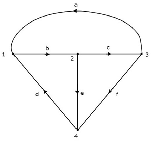
Directed Graph
If all the branches of a graph are represented with arrows, then that graph is called as a directed graph. These arrows indicate the direction of current flow in each branch. Hence, this graph is also called as oriented graph.
Consider the graph shown in the following figure.
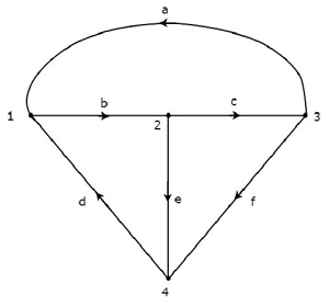
In the above graph, the direction of current flow is represented with an arrow in each branch. Hence, it is a directed graph.
Undirected Graph
If the branches of a graph are not represented with arrows, then that graph is called as an undirected graph. Since, there are no directions of current flow, this graph is also called as an unoriented graph.
The graph that was shown in the first Example of this chapter is an unoriented graph, because there are no arrows on the branches of that graph.
Subgraph and its Types
A part of the graph is called as a subgraph. We get subgraphs by removing some nodes and/or branches of a given graph. So, the number of branches and/or nodes of a subgraph will be less than that of the original graph. Hence, we can conclude that a subgraph is a subset of a graph.
Following are the two types of subgraphs.
- Tree
- Co-Tree
Tree
Tree is a connected subgraph of a given graph, which contains all the nodes of a graph. But, there should not be any loop in that subgraph. The branches of a tree are called as twigs.
Consider the following connected subgraph of the graph, which is shown in the Example of the beginning of this chapter.
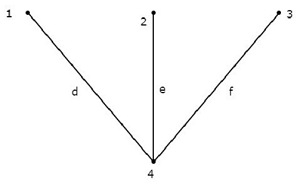
This connected subgraph contains all the four nodes of the given graph and there is no loop. Hence, it is a Tree.
This Tree has only three branches out of six branches of given graph. Because, if we consider even single branch of the remaining branches of the graph, then there will be a loop in the above connected subgraph. Then, the resultant connected subgraph will not be a Tree.
From the above Tree, we can conclude that the number of branches that are present in a Tree should be equal to n - 1 where ‘n’ is the number of nodes of the given graph.
Co-Tree
Co-Tree is a subgraph, which is formed with the branches that are removed while forming a Tree. Hence, it is called as Complement of a Tree. For every Tree, there will be a corresponding Co-Tree and its branches are called as links or chords. In general, the links are represented with dotted lines.
The Co-Tree corresponding to the above Tree is shown in the following figure.
This Co-Tree has only three nodes instead of four nodes of the given graph, because Node 4 is isolated from the above Co-Tree. Therefore, the Co-Tree need not be a connected subgraph. This Co-Tree has three branches and they form a loop.
The number of branches that are present in a co-tree will be equal to the difference between the number of branches of a given graph and the number of twigs. Mathematically, it can be written as
$$l = b - (n - 1)$$
$$l = b - n + 1$$
Where,
- l is the number of links.
- b is the number of branches present in a given graph.
- n is the number of nodes present in a given graph.
If we combine a Tree and its corresponding Co-Tree, then we will get the original graph as shown below.
The Tree branches d, e & f are represented with solid lines. The Co-Tree branches a, b & c are represented with dashed lines.
Network Topology Matrices
In the previous chapter, we discussed how to convert an electric circuit into an equivalent graph. Now, let us discuss the Network Topology Matrices which are useful for solving any electric circuit or network problem by using their equivalent graphs.
Matrices Associated with Network Graphs
Following are the three matrices that are used in Graph theory.
- Incidence Matrix
- Fundamental Loop Matrix
- Fundamental Cut set Matrix
Incidence Matrix
An Incidence Matrix represents the graph of a given electric circuit or network. Hence, it is possible to draw the graph of that same electric circuit or network from the incidence matrix.
We know that graph consists of a set of nodes and those are connected by some branches. So, the connecting of branches to a node is called as incidence. Incidence matrix is represented with the letter A. It is also called as node to branch incidence matrix or node incidence matrix.
If there are ‘n’ nodes and ‘b’ branches are present in a directed graph, then the incidence matrix will have ‘n’ rows and ‘b’ columns. Here, rows and columns are corresponding to the nodes and branches of a directed graph. Hence, the order of incidence matrix will be n × b.
The elements of incidence matrix will be having one of these three values, +1, -1 and 0.
If the branch current is leaving from a selected node, then the value of the element will be +1.
If the branch current is entering towards a selected node, then the value of the element will be -1.
If the branch current neither enters at a selected node nor leaves from a selected node, then the value of element will be 0.
Procedure to find Incidence Matrix
Follow these steps in order to find the incidence matrix of directed graph.
Select a node at a time of the given directed graph and fill the values of the elements of incidence matrix corresponding to that node in a row.
Repeat the above step for all the nodes of the given directed graph.
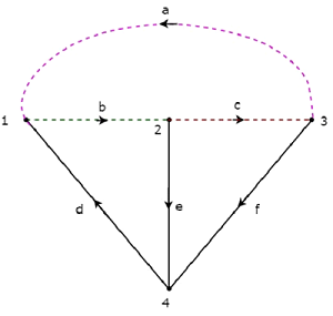
Example
Consider the following directed graph.
The incidence matrix corresponding to the above directed graph will be
$$A = \begin{bmatrix}-1 & 1 & 0 & -1 & 0 & 0\\0 & -1 & 1 & 0 & 1 & 0\\1 & 0 & -1 & 0 & 0 & 1 \\0 & 0 & 0 & 1 & -1 & -1 \end{bmatrix}$$
The rows and columns of the above matrix represents the nodes and branches of given directed graph. The order of this incidence matrix is 4 × 6.
By observing the above incidence matrix, we can conclude that the summation of column elements of incidence matrix is equal to zero. That means, a branch current leaves from one node and enters at another single node only.
Note − If the given graph is an un-directed type, then convert it into a directed graph by representing the arrows on each branch of it. We can consider the arbitrary direction of current flow in each branch.
Fundamental Loop Matrix
Fundamental loop or f-loop is a loop, which contains only one link and one or more twigs. So, the number of f-loops will be equal to the number of links. Fundamental loop matrix is represented with letter B. It is also called as fundamental circuit matrix and Tie-set matrix. This matrix gives the relation between branch currents and link currents.
If there are ‘n’ nodes and ‘b’ branches are present in a directed graph, then the number of links present in a co-tree, which is corresponding to the selected tree of given graph will be b-n+1.
So, the fundamental loop matrix will have ‘b-n+1’ rows and ‘b’ columns. Here, rows and columns are corresponding to the links of co-tree and branches of given graph. Hence, the order of fundamental loop matrix will be (b - n + 1) × b.
The elements of fundamental loop matrix will be having one of these three values, +1, -1 and 0.
The value of element will be +1 for the link of selected f-loop.
The value of elements will be 0 for the remaining links and twigs, which are not part of the selected f-loop.
If the direction of twig current of selected f-loop is same as that of f-loop link current, then the value of element will be +1.
If the direction of twig current of selected f-loop is opposite to that of f-loop link current, then the value of element will be -1.
Procedure to find Fundamental Loop Matrix
Follow these steps in order to find the fundamental loop matrix of given directed graph.
Select a tree of given directed graph.
By including one link at a time, we will get one f-loop. Fill the values of elements corresponding to this f-loop in a row of fundamental loop matrix.
Repeat the above step for all links.
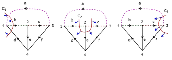
Example
Take a look at the following Tree of directed graph, which is considered for incidence matrix.
The above Tree contains three branches d, e & f. Hence, the branches a, b & c will be the links of the Co-Tree corresponding to the above Tree. By including one link at a time to the above Tree, we will get one f-loop. So, there will be three f-loops, since there are three links. These three f-loops are shown in the following figure.
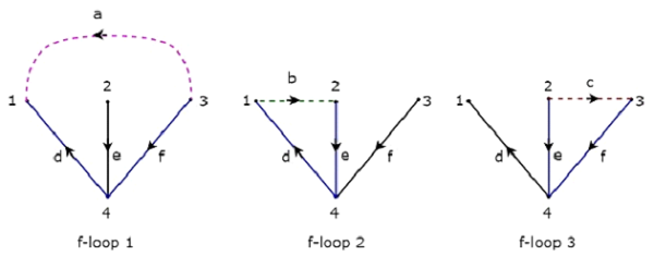
In the above figure, the branches, which are represented with colored lines form f-loops. We will get the row wise element values of Tie-set matrix from each f-loop. So, the Tieset matrix of the above considered Tree will be
$$B = \begin{bmatrix}1 & 0 & 0 & -1 & 0 & -1\\0 & 1 & 0 & 1 & 1 & 0\\0 & 0 & 1 & 0 & -1 & 1 \end{bmatrix}$$
The rows and columns of the above matrix represents the links and branches of given directed graph. The order of this incidence matrix is 3 × 6.
The number of Fundamental loop matrices of a directed graph will be equal to the number of Trees of that directed graph. Because, every Tree will be having one Fundamental loop matrix.
Fundamental Cut-set Matrix
Fundamental cut set or f-cut set is the minimum number of branches that are removed from a graph in such a way that the original graph will become two isolated subgraphs. The f-cut set contains only one twig and one or more links. So, the number of f-cut sets will be equal to the number of twigs.
Fundamental cut set matrix is represented with letter C. This matrix gives the relation between branch voltages and twig voltages.
If there are ‘n’ nodes and ‘b’ branches are present in a directed graph, then the number of twigs present in a selected Tree of given graph will be n-1. So, the fundamental cut set matrix will have ‘n-1’ rows and ‘b’ columns. Here, rows and columns are corresponding to the twigs of selected tree and branches of given graph. Hence, the order of fundamental cut set matrix will be (n-1) × b.
The elements of fundamental cut set matrix will be having one of these three values, +1, -1 and 0.
The value of element will be +1 for the twig of selected f-cutset.
The value of elements will be 0 for the remaining twigs and links, which are not part of the selected f-cutset.
If the direction of link current of selected f-cut set is same as that of f-cutset twig current, then the value of element will be +1.
If the direction of link current of selected f-cut set is opposite to that of f-cutset twig current, then the value of element will be -1.
Procedure to find Fundamental Cut-set Matrix
Follow these steps in order to find the fundamental cut set matrix of given directed graph.
Select a Tree of given directed graph and represent the links with the dotted lines.
By removing one twig and necessary links at a time, we will get one f-cut set. Fill the values of elements corresponding to this f-cut set in a row of fundamental cut set matrix.
Repeat the above step for all twigs.
Example
Consider the same directed graph , which we discussed in the section of incidence matrix. Select the branches d, e & f of this directed graph as twigs. So, the remaining branches a, b & c of this directed graph will be the links.
The twigs d, e & f are represented with solid lines and links a, b & c are represented with dotted lines in the following figure.
By removing one twig and necessary links at a time, we will get one f-cut set. So, there will be three f-cut sets, since there are three twigs. These three f-cut sets are shown in the following figure.
We will be having three f-cut sets by removing a set of twig and links of C1, C2 and C3. We will get the row wise element values of fundamental cut set matrix from each f-cut set. So, the fundamental cut set matrix of the above considered Tree will be
$$C = \begin{bmatrix}1 & -1 & 0 & 1 & 0 & 0\\0 & -1 & 1 & 0 & 1 & 0\\1 & 0 & -1 & 0 & 0 & 1 \end{bmatrix}$$
The rows and columns of the above matrix represents the twigs and branches of given directed graph. The order of this fundamental cut set matrix is 3 × 6.
The number of Fundamental cut set matrices of a directed graph will be equal to the number of Trees of that directed graph. Because, every Tree will be having one Fundamental cut set matrix.
Network Theory - Superposition Theorem
Superposition theorem is based on the concept of linearity between the response and excitation of an electrical circuit. It states that the response in a particular branch of a linear circuit when multiple independent sources are acting at the same time is equivalent to the sum of the responses due to each independent source acting at a time.
In this method, we will consider only one independent source at a time. So, we have to eliminate the remaining independent sources from the circuit. We can eliminate the voltage sources by shorting their two terminals and similarly, the current sources by opening their two terminals.
Therefore, we need to find the response in a particular branch ‘n’ times if there are ‘n’ independent sources. The response in a particular branch could be either current flowing through that branch or voltage across that branch.
Procedure of Superposition Theorem
Follow these steps in order to find the response in a particular branch using superposition theorem.
Step 1 − Find the response in a particular branch by considering one independent source and eliminating the remaining independent sources present in the network.
Step 2 − Repeat Step 1 for all independent sources present in the network.
Step 3 − Add all the responses in order to get the overall response in a particular branch when all independent sources are present in the network.
Example
Find the current flowing through 20 Ω resistor of the following circuit using superposition theorem.
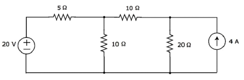
Step 1 − Let us find the current flowing through 20 Ω resistor by considering only 20 V voltage source. In this case, we can eliminate the 4 A current source by making open circuit of it. The modified circuit diagram is shown in the following figure.
There is only one principal node except Ground in the above circuit. So, we can use nodal analysis method. The node voltage V1 is labelled in the following figure. Here, V1 is the voltage from node 1 with respect to ground.
The nodal equation at node 1 is
$$\frac{V_1 - 20}{5} + \frac{V_1}{10} + \frac{V_1}{10 + 20} = 0$$
$$\Rightarrow \frac{6V_1 - 120 + 3V_1 + V_1}{30} = 0$$
$$\Rightarrow 10V_1 = 120$$
$$\Rightarrow V_1 = 12V$$
The current flowing through 20 Ω resistor can be found by doing the following simplification.
$$I_1 = \frac{V_1}{10 + 20}$$
Substitute the value of V1 in the above equation.
$$I_1 = \frac{12}{10 + 20} = \frac{12}{30} = 0.4 A$$
Therefore, the current flowing through 20 Ω resistor is 0.4 A, when only 20 V voltage source is considered.
Step 2 − Let us find the current flowing through 20 Ω resistor by considering only 4 A current source. In this case, we can eliminate the 20 V voltage source by making short-circuit of it. The modified circuit diagram is shown in the following figure.
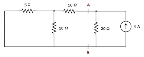
In the above circuit, there are three resistors to the left of terminals A & B. We can replace these resistors with a single equivalent resistor. Here, 5 Ω & 10 Ω resistors are connected in parallel and the entire combination is in series with 10 Ω resistor.
The equivalent resistance to the left of terminals A & B will be
$$R_{AB} = \lgroup \frac{5 \times 10}{5 + 10} \rgroup + 10 = \frac{10}{3} + 10 = \frac{40}{3} \Omega$$
The simplified circuit diagram is shown in the following figure.
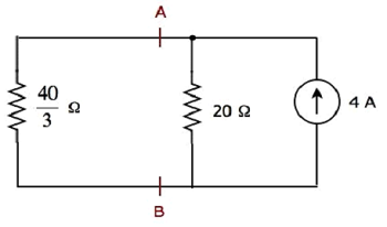
We can find the current flowing through 20 Ω resistor, by using current division principle.
$$I_2 = I_S \lgroup \frac{R_1}{R_1 + R_2} \rgroup$$
Substitute $I_S = 4A,\: R_1 = \frac{40}{3} \Omega$ and $R_2 = 20 \Omega$ in the above equation.
$$I_2 = 4 \lgroup \frac{\frac{40}{3}}{\frac{40}{3} + 20} \rgroup = 4 \lgroup \frac{40}{100} \rgroup = 1.6 A$$
Therefore, the current flowing through 20 Ω resistor is 1.6 A, when only 4 A current source is considered.
Step 3 − We will get the current flowing through 20 Ω resistor of the given circuit by doing the addition of two currents that we got in step 1 and step 2. Mathematically, it can be written as
$$I = I_1 + I_2$$
Substitute, the values of I1 and I2 in the above equation.
$$I = 0.4 + 1.6 = 2 A$$
Therefore, the current flowing through 20 Ω resistor of given circuit is 2 A.
Note − We can’t apply superposition theorem directly in order to find the amount of power delivered to any resistor that is present in a linear circuit, just by doing the addition of powers delivered to that resistor due to each independent source. Rather, we can calculate either total current flowing through or voltage across that resistor by using superposition theorem and from that, we can calculate the amount of power delivered to that resistor using $I^2 R$ or $\frac{V^2}{R}$.
Network Theory - Thevenin’s Theorem
Thevenin’s theorem states that any two terminal linear network or circuit can be represented with an equivalent network or circuit, which consists of a voltage source in series with a resistor. It is known as Thevenin’s equivalent circuit. A linear circuit may contain independent sources, dependent sources, and resistors.
If the circuit contains multiple independent sources, dependent sources, and resistors, then the response in an element can be easily found by replacing the entire network to the left of that element with a Thevenin’s equivalent circuit.
The response in an element can be the voltage across that element, current flowing through that element, or power dissipated across that element.
This concept is illustrated in following figures.
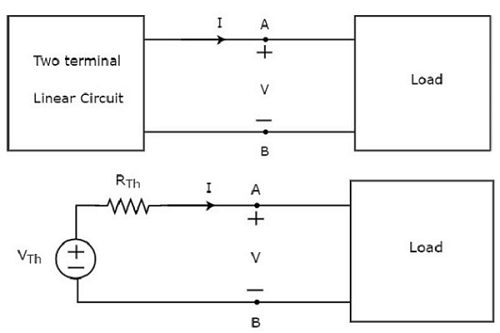
Thevenin’s equivalent circuit resembles a practical voltage source. Hence, it has a voltage source in series with a resistor.
The voltage source present in the Thevenin’s equivalent circuit is called as Thevenin’s equivalent voltage or simply Thevenin’s voltage, VTh.
The resistor present in the Thevenin’s equivalent circuit is called as Thevenin’s equivalent resistor or simply Thevenin’s resistor, RTh.
Methods of Finding Thevenin’s Equivalent Circuit
There are three methods for finding a Thevenin’s equivalent circuit. Based on the type of sources that are present in the network, we can choose one of these three methods. Now, let us discuss two methods one by one. We will discuss the third method in the next chapter.
Method 1
Follow these steps in order to find the Thevenin’s equivalent circuit, when only the sources of independent type are present.
Step 1 − Consider the circuit diagram by opening the terminals with respect to which the Thevenin’s equivalent circuit is to be found.
Step 2 − Find Thevenin’s voltage VTh across the open terminals of the above circuit.
Step 3 − Find Thevenin’s resistance RTh across the open terminals of the above circuit by eliminating the independent sources present in it.
Step 4 − Draw the Thevenin’s equivalent circuit by connecting a Thevenin’s voltage VTh in series with a Thevenin’s resistance RTh.
Now, we can find the response in an element that lies to the right side of Thevenin’s equivalent circuit.
Example
Find the current flowing through 20 Ω resistor by first finding a Thevenin’s equivalent circuit to the left of terminals A and B.
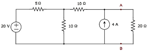
Step 1 − In order to find the Thevenin’s equivalent circuit to the left side of terminals A & B, we should remove the 20 Ω resistor from the network by opening the terminals A & B. The modified circuit diagram is shown in the following figure.
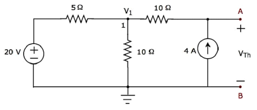
Step 2 − Calculation of Thevenin’s voltage VTh.
There is only one principal node except Ground in the above circuit. So, we can use nodal analysis method. The node voltage V1 and Thevenin’s voltage VTh are labelled in the above figure. Here, V1 is the voltage from node 1 with respect to Ground and VTh is the voltage across 4 A current source.
The nodal equation at node 1 is
$$\frac{V_1 - 20}{5} + \frac{V_1}{10} - 4 = 0$$
$$\Rightarrow \frac{2V_1 - 40 + V_1 - 40}{10} = 0$$
$$\Rightarrow 3V_1 - 80 = 0$$
$$\Rightarrow V_1 = \frac{80}{3}V$$
The voltage across series branch 10 Ω resistor is
$$V_{10 \Omega} = (-4)(10) = -40V$$
There are two meshes in the above circuit. The KVL equation around second mesh is
$$V_1 - V_{10 \Omega} - V_{Th} = 0$$
Substitute the values of $V_1$ and $V_{10 \Omega}$ in the above equation.
$$\frac{80}{3} - (-40) - V_{Th} = 0$$
$$V_{Th} = \frac{80 + 120}{3} = \frac{200}{3}V$$
Therefore, the Thevenin’s voltage is $V_{Th} = \frac{200}{3}V$
Step 3 − Calculation of Thevenin’s resistance RTh.
Short circuit the voltage source and open circuit the current source of the above circuit in order to calculate the Thevenin’s resistance RTh across the terminals A & B. The modified circuit diagram is shown in the following figure.
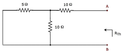
The Thevenin’s resistance across terminals A & B will be
$$R_{Th} = \lgroup \frac{5 \times 10}{5 + 10} \rgroup + 10 = \frac{10}{3} + 10 = \frac{40}{3} \Omega$$
Therefore, the Thevenin’s resistance is $\mathbf {R_{Th} = \frac{40}{3} \Omega}$.
Step 4 − The Thevenin’s equivalent circuit is placed to the left of terminals A & B in the given circuit. This circuit diagram is shown in the following figure.
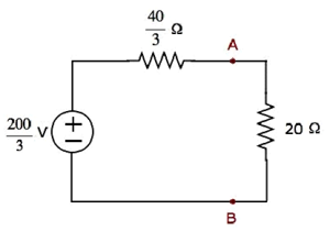
The current flowing through the 20 Ω resistor can be found by substituting the values of VTh, RTh and R in the following equation.
$$l = \frac{V_{Th}}{R_{Th} + R}$$
$$l = \frac{\frac{200}{3}}{\frac{40}{3} + 20} = \frac{200}{100} = 2A$$
Therefore, the current flowing through the 20 Ω resistor is 2 A.
Method 2
Follow these steps in order to find the Thevenin’s equivalent circuit, when the sources of both independent type and dependent type are present.
Step 1 − Consider the circuit diagram by opening the terminals with respect to which, the Thevenin’s equivalent circuit is to be found.
Step 2 − Find Thevenin’s voltage VTh across the open terminals of the above circuit.
Step 3 − Find the short circuit current ISC by shorting the two opened terminals of the above circuit.
Step 4 − Find Thevenin’s resistance RTh by using the following formula.
$$R_{Th} = \frac{V_{Th}}{I_{SC}}$$
Step 5 − Draw the Thevenin’s equivalent circuit by connecting a Thevenin’s voltage VTh in series with a Thevenin’s resistance RTh.
Now, we can find the response in an element that lies to the right side of the Thevenin’s equivalent circuit.
Network Theory - Norton’s Theorem
Norton’s theorem is similar to Thevenin’s theorem. It states that any two terminal linear network or circuit can be represented with an equivalent network or circuit, which consists of a current source in parallel with a resistor. It is known as Norton’s equivalent circuit. A linear circuit may contain independent sources, dependent sources and resistors.
If a circuit has multiple independent sources, dependent sources, and resistors, then the response in an element can be easily found by replacing the entire network to the left of that element with a Norton’s equivalent circuit.
The response in an element can be the voltage across that element, current flowing through that element or power dissipated across that element.
This concept is illustrated in following figures.
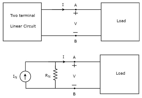
Norton’s equivalent circuit resembles a practical current source. Hence, it is having a current source in parallel with a resistor.
The current source present in the Norton’s equivalent circuit is called as Norton’s equivalent current or simply Norton’s current IN.
The resistor present in the Norton’s equivalent circuit is called as Norton’s equivalent resistor or simply Norton’s resistor RN.
Methods of Finding Norton’s Equivalent Circuit
There are three methods for finding a Norton’s equivalent circuit. Based on the type of sources that are present in the network, we can choose one of these three methods. Now, let us discuss these three methods one by one.
Method 1
Follow these steps in order to find the Norton’s equivalent circuit, when only the sources of independent type are present.
Step 1 − Consider the circuit diagram by opening the terminals with respect to which, the Norton’s equivalent circuit is to be found.
Step 2 − Find the Norton’s current IN by shorting the two opened terminals of the above circuit.
Step 3 − Find the Norton’s resistance RN across the open terminals of the circuit considered in Step1 by eliminating the independent sources present in it. Norton’s resistance RN will be same as that of Thevenin’s resistance RTh.
Step 4 − Draw the Norton’s equivalent circuit by connecting a Norton’s current IN in parallel with Norton’s resistance RN.
Now, we can find the response in an element that lies to the right side of Norton’s equivalent circuit.
Method 2
Follow these steps in order to find the Norton’s equivalent circuit, when the sources of both independent type and dependent type are present.
Step 1 − Consider the circuit diagram by opening the terminals with respect to which the Norton’s equivalent circuit is to be found.
Step 2 − Find the open circuit voltage VOC across the open terminals of the above circuit.
Step 3 − Find the Norton’s current IN by shorting the two opened terminals of the above circuit.
Step 4 − Find Norton’s resistance RN by using the following formula.
$$R_N = \frac{V_{OC}}{I_N}$$
Step 5 − Draw the Norton’s equivalent circuit by connecting a Norton’s current IN in parallel with Norton’s resistance RN.
Now, we can find the response in an element that lies to the right side of Norton’s equivalent circuit.
Method 3
This is an alternate method for finding a Norton’s equivalent circuit.
Step 1 − Find a Thevenin’s equivalent circuit between the desired two terminals. We know that it consists of a Thevenin’s voltage source, VTh and Thevenin’s resistor, RTh.
Step 2 − Apply source transformation technique to the above Thevenin’s equivalent circuit. We will get the Norton’s equivalent circuit. Here,
Norton’s current,
$$I_N = \frac{V_{Th}}{R_{Th}}$$
Norton’s resistance,
$$R_N = R_{Th}$$
This concept is illustrated in the following figure.
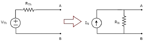
Now, we can find the response in an element by placing Norton’s equivalent circuit to the left of that element.
Note − Similarly, we can find the Thevenin’s equivalent circuit by finding a Norton’s equivalent circuit first and then apply source transformation technique to it. This concept is illustrated in the following figure.
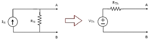
This is the Method 3 for finding a Thevenin’s equivalent circuit.
Example
Find the current flowing through 20 Ω resistor by first finding a Norton’s equivalent circuit to the left of terminals A and B.

Let us solve this problem using Method 3.
Step 1 − In previous chapter, we calculated the Thevenin’s equivalent circuit to the left side of terminals A & B. We can use this circuit now. It is shown in the following figure.
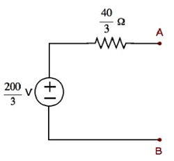
Here, Thevenin’s voltage, $V_{Th} = \frac{200}{3} V$ and Thevenin’s resistance, $R_{Th} = \frac{40}{3} \Omega$
Step 2 − Apply source transformation technique to the above Thevenin’s equivalent circuit. Substitute the values of VTh and RTh in the following formula of Norton’s current.
$$I_N = \frac{V_{Th}}{R_{Th}}$$
$$I_N = \frac{\frac{200}{3}}{\frac{40}{3}} = 5A$$
Therefore, Norton’s current IN is 5 A.
We know that Norton’s resistance, RN is same as that of Thevenin’s resistance RTh.
$$\mathbf {R_N = \frac{40}{3} \Omega}$$
The Norton’s equivalent circuit corresponding to the above Thevenin’s equivalent circuit is shown in the following figure.
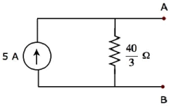
Now, place the Norton’s equivalent circuit to the left of the terminals A & B of the given circuit.
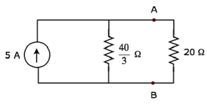
By using current division principle, the current flowing through the 20 Ω resistor will be
$$I_{20 \Omega} = 5 \lgroup \frac{\frac{40}{3}}{\frac{40}{3} + 20} \rgroup$$
$$I_{20 \Omega} = 5 \lgroup \frac{40}{100} \rgroup = 2A$$
Therefore, the current flowing through the 20 Ω resistor is 2 A.
Maximum Power Transfer Theorem
The amount of power received by a load is an important parameter in electrical and electronic applications. In DC circuits, we can represent the load with a resistor having resistance of RL ohms. Similarly, in AC circuits, we can represent it with a complex load having an impedance of ZL ohms.
Maximum power transfer theorem states that the DC voltage source will deliver maximum power to the variable load resistor only when the load resistance is equal to the source resistance.
Similarly, Maximum power transfer theorem states that the AC voltage source will deliver maximum power to the variable complex load only when the load impedance is equal to the complex conjugate of source impedance.
In this chapter, let us discuss about the maximum power transfer theorem for DC circuits.
Proof of Maximum Power Transfer Theorem
Replace any two terminal linear network or circuit to the left side of variable load resistor having resistance of RL ohms with a Thevenin’s equivalent circuit. We know that Thevenin’s equivalent circuit resembles a practical voltage source.
This concept is illustrated in following figures.
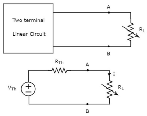
The amount of power dissipated across the load resistor is
$$P_L = I^2 R_L$$
Substitute $I = \frac{V_{Th}}{R_{Th} + R_L}$ in the above equation.
$$P_L = \lgroup \frac{V_{Th}}{(R_{Th} + R_L)} \rgroup ^2 R_L$$
$\Rightarrow P_L = {V_{Th}}^2 \lbrace \frac{R_L}{(R_{Th} + R_L)^2} \rbrace$ Equation 1
Condition for Maximum Power Transfer
For maximum or minimum, first derivative will be zero. So, differentiate Equation 1 with respect to RL and make it equal to zero.
$$\frac{dP_L}{dR_L} = {V_{Th}}^2 \lbrace \frac{(R_{Th} + R_L)^2 \times 1 - R_L \times 2(R_{Th} + R_L)}{(R_{Th} + R_L)^4} \rbrace = 0$$
$$\Rightarrow (R_{Th} + R_L)^2 -2R_L(R_{Th} + R_L) = 0$$
$$\Rightarrow (R_{Th} + R_L)(R_{Th} + R_L - 2R_L) = 0$$
$$\Rightarrow (R_{Th} - R_L) = 0$$
$$\Rightarrow R_{Th} = R_L\:or\:R_L = R_{Th}$$
Therefore, the condition for maximum power dissipation across the load is $R_L = R_{Th}$. That means, if the value of load resistance is equal to the value of source resistance i.e., Thevenin’s resistance, then the power dissipated across the load will be of maximum value.
The value of Maximum Power Transfer
Substitute $R_L = R_{Th}\:\&\:P_L = P_{L, Max}$ in Equation 1.
$$P_{L, Max} = {V_{Th}}^2 \lbrace \frac{R_{Th}}{(R_{Th} + R_{Th})^2} \rbrace$$
$$P_{L, Max} = {V_{Th}}^2 \lbrace \frac{R_{Th}}{4 {R_{Th}}^2} \rbrace$$
$$\Rightarrow P_{L, Max} = \frac{{V_{Th}}^2}{4 R_{Th}}$$
$$\Rightarrow P_{L, Max} = \frac{{V_{Th}}^2}{4 R_{L}}, \: since \: R_{L} = R_{Th}$$
Therefore, the maximum amount of power transferred to the load is
$$P_{L, Max} = \frac{{V_{Th}}^2}{4R_{L}} = \frac{{V_{Th}}^2}{4R_{Th}}$$
Efficiency of Maximum Power Transfer
We can calculate the efficiency of maximum power transfer, $\eta_{Max}$ using following formula.
$\eta_{Max} = \frac{P_{L, Max}}{P_S}$ Equation 2
Where,
$P_{L, Max}$ is the maximum amount of power transferred to the load.
$P_S$ is the amount of power generated by the source.
The amount of power generated by the source is
$$P_S = I^2 R_{Th} + I^2 R_L$$
$$\Rightarrow P_S = 2 I^2 R_{Th},\:since\:R_{L} = R_{Th}$$
Substitute $I = \frac{V_{Th}}{2 R_{Th}}$ in the above equation.
$$P_S = 2\lgroup \frac{V_{Th}}{2 R_{Th}} \rgroup ^2 R_{Th}$$
$$\Rightarrow P_S = 2\lgroup \frac{{V_{Th}}^2}{4 {R_{Th}}^2} \rgroup R_{Th}$$
$$\Rightarrow P_S = \frac{{V_{Th}}^2}{2 R_{Th}}$$
Substitute the values of $P_{L, Max}$ and $P_S$ in Equation 2.
$$\eta_{Max} = \frac{\lgroup \frac{{V_{Th}}^2}{4R_{Th}} \rgroup}{\lgroup \frac{{V_{Th}}^2}{2R_{Th}}\rgroup}$$
$$\Rightarrow \eta_{Max} = \frac{1}{2}$$
We can represent the efficiency of maximum power transfer in terms of percentage as follows −
$$\% \eta_{Max} = \eta_{Max} \times 100\%$$
$$\Rightarrow \% \eta_{Max} = \lgroup \frac{1}{2} \rgroup \times 100\%$$
$$\Rightarrow \% \eta_{Max} = 50\%$$
Therefore, the efficiency of maximum power transfer is 50 %.
Example
Find the maximum power that can be delivered to the load resistor RL of the circuit shown in the following figure.
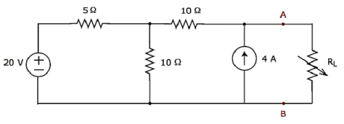
Step 1 − In Thevenin’s Theorem chapter, we calculated the Thevenin’s equivalent circuit to the left side of terminals A & B. We can use this circuit now. It is shown in the following figure.
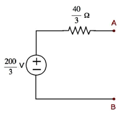
Here, Thevenin’s voltage $V_{Th} = \frac{200}{3}V$ and Thevenin’s resistance $R_{Th} = \frac{40}{3} \Omega$
Step 2 − Replace the part of the circuit, which is left side of terminals A & B of the given circuit with the above Thevenin’s equivalent circuit. The resultant circuit diagram is shown in the following figure.
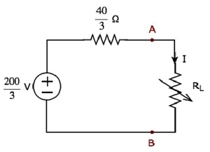
Step 3 − We can find the maximum power that will be delivered to the load resistor, RL by using the following formula.
$$P_{L, Max} = \frac{{V_{Th}}^2}{4 R_{Th}}$$
Substitute $V_{Th} = \frac{200}{3}V$ and $R_{Th} = \frac{40}{3} \Omega$ in the above formula.
$$P_{L, Max} = \frac{\lgroup \frac{200}{3} \rgroup ^ 2}{4 \lgroup \frac{40}{3}\rgroup } $$
$$P_{L, Max} = \frac{250}{3} W$$
Therefore, the maximum power that will be delivered to the load resistor RL of the given circuit is $\mathbf {\frac{250}{3}}$ W
Network Theory - Response of DC Circuits
If the output of an electric circuit for an input varies with respect to time, then it is called as time response. The time response consists of following two parts.
- Transient Response
- Steady state Response
In this chapter, first let us discuss about these two responses and then observe these two responses in a series RL circuit, when it is excited by a DC voltage source.
Transient Response
After applying an input to an electric circuit, the output takes certain time to reach steady state. So, the output will be in transient state till it goes to a steady state. Therefore, the response of the electric circuit during the transient state is known as transient response.
The transient response will be zero for large values of ‘t’. Ideally, this value of ‘t’ should be infinity. But, practically five time constants are sufficient.
Presence or Absence of Transients
Transients occur in the response due to sudden change in the sources that are applied to the electric circuit and / or due to switching action. There are two possible switching actions. Those are opening switch and closing switch.
The transient part will not present in the response of an electrical circuit or network, if it contains only resistances. Because resistor is having the ability to adjust any amount of voltage and current.
The transient part occurs in the response of an electrical circuit or network due to the presence of energy storing elements such as inductor and capacitor. Because they can’t change the energy stored in those elements instantly.
Inductor Behavior
Assume the switching action takes place at t = 0. Inductor current does not change instantaneously, when the switching action takes place. That means, the value of inductor current just after the switching action will be same as that of just before the switching action.
Mathematically, it can be represented as
$$i_L (0^+) = i_L (0^-)$$
Capacitor Behavior
The capacitor voltage does not change instantaneously similar to the inductor current, when the switching action takes place. That means, the value of capacitor voltage just after the switching action will be same as that of just before the switching action.
Mathematically, it can be represented as
$$v_c (0^+) = v_c (0^-)$$
Steady state Response
The part of the time response that remains even after the transient response has become zero value for large values of ‘t’ is known as steady state response. This means, there won’t be any transient part in the response during steady state.
Inductor Behavior
If the independent source is connected to the electric circuit or network having one or more inductors and resistors (optional) for a long time, then that electric circuit or network is said to be in steady state. Therefore, the energy stored in the inductor(s) of that electric circuit is of maximum and constant.
Mathematically, it can be represented as
$W_L = \frac{L {i_L}^2}{2} = $ Maximum & constant
$\Rightarrow i_L = $ Maximum & constant
Therefore, inductor acts as a constant current source in steady state.
The voltage across inductor will be
$$V_L = L \frac{di_{L}}{dt} = 0V$$
So, the inductor acts as a short circuit in steady state.
Capacitor Behavior
If the independent source is connected to the electric circuit or network having one or more capacitors and resistors (optional) for a long time, then that electric circuit or network is said to be in steady state. Therefore, the energy stored in the capacitor(s) of that electric circuit is of maximum and constant.
Mathematically, it can be represented as
$W_c = \frac{C{v_c}^2}{2} = $ Maximum & constant
$\Rightarrow v_c = $Maximum & constant
Therefore, capacitor acts as a constant voltage source in steady state.
The current flowing through the capacitor will be
$$i_c = C\frac{dv_c}{dt} = 0A$$
So, the capacitor acts as an open circuit in steady state.
Finding the Response of Series RL Circuit
Consider the following series RL circuit diagram.
In the above circuit, the switch was kept open up to t = 0 and it was closed at t = 0. So, the DC voltage source having V volts is not connected to the series RL circuit up to this instant. Therefore, there is no initial current flows through inductor.
The circuit diagram, when the switch is in closed position is shown in the following figure.
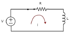
Now, the current i flows in the entire circuit, since the DC voltage source having V volts is connected to the series RL circuit.
Now, apply KVL around the loop.
$$V = Ri + L \frac{di}{dt}$$
$\frac{di}{dt} + \lgroup \frac{R}{L} \rgroup i = \frac{V}{L}$Equation 1
The above equation is a first order differential equation and it is in the form of
$\frac{dy}{dt} + Py = Q$Equation 2
By comparing Equation 1 and Equation 2, we will get the following relations.
$$x = t$$
$$y = i$$
$$P = \frac{R}{L}$$
$$Q = \frac{V}{L}$$
The solution of Equation 2 will be
$ye^{\int p dx} = \int Q e^{\int p dx} dx + k$Equation 3
Where, k is the constant.
Substitute, the values of x, y, P & Q in Equation 3.
$ie^{\int {\lgroup \frac{R}{L} \rgroup}dt} = \int (\frac{V}{L}) \lgroup e^{\int {\lgroup \frac{R}{L} \rgroup}dt} \rgroup dt + k$
$\Rightarrow ie^{\lgroup \frac{R}{L} \rgroup t} = \frac{V}{L} \int e^{\lgroup \frac{R}{L} \rgroup t} dt + k$
$\Rightarrow ie^{\lgroup \frac{R}{L} \rgroup t} = \frac{V}{L} \lbrace \frac{e^{\lgroup \frac{R}{L} \rgroup}t}{\frac{R}{L}} \rbrace + k$
$\Rightarrow i = \frac{V}{R} + k e^{-\lgroup \frac{R}{L} \rgroup}t$Equation 4
We know that there is no initial current in the circuit. Hence, substitute, t = 0 and 𝑖 = 0 in Equation 4 in order to find the value of the constant k.
$$0 = \frac{V}{R} + ke^{-\lgroup \frac{R}{L} \rgroup(0)}$$
$$0 = \frac{V}{R} + k(1)$$
$$k = - \frac{V}{R}$$
Substitute, the value of k in Equation 4.
$$i = \frac{V}{R} + \lgroup - \frac{V}{R} \rgroup e^{-\lgroup \frac{R}{L} \rgroup t}$$
$$i = \frac{V}{R} - \frac{V}{R}e^{-\lgroup \frac{R}{L} \rgroup t}$$
Therefore, the current flowing through the circuit is
$i = - \frac{V}{R}e^{-\lgroup \frac{R}{L} \rgroup t} + \frac{V}{R}$Equation 5
So, the response of the series RL circuit, when it is excited by a DC voltage source, has the following two terms.
The first term $-\frac{V}{R}e^{-\lgroup \frac{R}{L} \rgroup t}$ corresponds with the transient response.
The second term $\frac{V}{R}$ corresponds with the steady state response. These two responses are shown in the following figure.
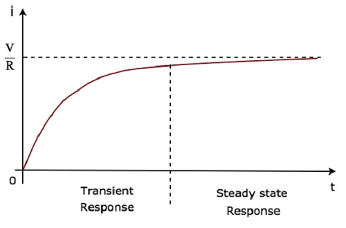
We can re-write the Equation 5 as follows −
$i = \frac{V}{R} \lgroup 1 - e^{-\lgroup \frac{R}{L} \rgroup t} \rgroup$
$\Rightarrow i = \frac{V}{R} \lgroup 1 - e^{-\lgroup \frac{t}{\tau} \rgroup} \rgroup$Equation 6
Where, τ is the time constant and its value is equal to $\frac{L}{R}$.
Both Equation 5 and Equation 6 are same. But, we can easily understand the above waveform of current flowing through the circuit from Equation 6 by substituting a few values of t like 0, τ, 2τ, 5τ, etc.
In the above waveform of current flowing through the circuit, the transient response will present up to five time constants from zero, whereas the steady state response will present from five time constants onwards.
Network Theory - Response of AC Circuits
In the previous chapter, we discussed the transient response and steady state response of DC circuit. In this chapter, let us discuss the response of AC circuit. The concepts of both transient response and steady state response, which we discussed in the previous chapter, will be useful here too.
Finding the Response of Series RL Circuit
Consider the following series RL circuit diagram.
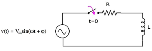
In the above circuit, the switch was kept open up to t = 0 and it was closed at t = 0. So, the AC voltage source having a peak voltage of Vm volts is not connected to the series RL circuit up to this instant. Therefore, there is no initial current flows through the inductor.
The circuit diagram, when the switch is in closed position, is shown in the following figure.
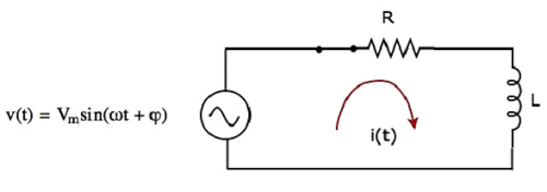
Now, the current i(t) flows in the entire circuit, since the AC voltage source having a peak voltage of Vm volts is connected to the series RL circuit.
We know that the current i(t) flowing through the above circuit will have two terms, one that represents the transient part and other term represents the steady state.
Mathematically, it can be represented as
$i(t) = i_{Tr}(t) + i_{ss}(t)$Equation 1
Where,
$i_{Tr}(t)$ is the transient response of the current flowing through the circuit.
$i_{ss}(t)$ is the steady state response of the current flowing through the circuit.
In the previous chapter, we got the transient response of the current flowing through the series RL circuit. It is in the form of $Ke^{-\lgroup \frac{t}{\tau} \rgroup}$.
Substitute $i_{Tr}(t) = Ke^{-\lgroup \frac{t}{\tau} \rgroup}$ in Equation 1.
$i(t) = Ke^{-\lgroup \frac{t}{\tau} \rgroup} + i_{ss}(t)$Equation 2
Calculation of Steady State Current
If a sinusoidal signal is applied as an input to a Linear electric circuit, then it produces a steady state output, which is also a sinusoidal signal. Both the input and output sinusoidal signals will be having the same frequency, but different amplitudes and phase angles.
We can calculate the steady state response of an electric circuit, when it is excited by a sinusoidal voltage source using Laplace Transform approach.
The s-domain circuit diagram, when the switch is in closed position, is shown in the following figure.
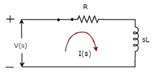
In the above circuit, all the quantities and parameters are represented in s-domain. These are the Laplace transforms of time-domain quantities and parameters.
The Transfer function of the above circuit is
$$H(s) = \frac{I(s)}{V(s)}$$
$$\Rightarrow H(s) = \frac{1}{Z(s)}$$
$$\Rightarrow H(s) = \frac{1}{R + sL}$$
Substitute $s = j \omega$ in the above equation.
$$H(j \omega) = \frac{1}{R + j \omega L}$$
Magnitude of $\mathbf{\mathit{H(j \omega)}}$ is
$$|H(j \omega)| = \frac{1}{\sqrt{R^2 + {\omega}^2}L^2}$$
Phase angle of $\mathbf{\mathit{H(j \omega)}}$ is
$$\angle H(j \omega) = -tan^{-1} \lgroup \frac{\omega L}{R} \rgroup$$
We will get the steady state current $i_{ss}(t)$ by doing the following two steps −
Multiply the peak voltage of input sinusoidal voltage and the magnitude of $H(j \omega)$.
Add the phase angles of input sinusoidal voltage and $H(j \omega)$.
The steady state current $i_{ss}(t)$ will be
$$i_{ss}(t) = \frac{V_m}{\sqrt{R^2 +{\omega}^2 L^2}} sin \lgroup \omega t + \varphi - tan^{-1} \lgroup \frac {\omega L}{R}\rgroup \rgroup$$
Substitute the value of $i_{ss}(t)$ in Equation 2.
$i(t) = Ke^{-\lgroup \frac{t}{\tau} \rgroup} + \frac{V_m}{\sqrt{R^2 +{\omega}^2 L^2}} sin \lgroup \omega t + \varphi - tan^{-1} \lgroup \frac {\omega L}{R}\rgroup \rgroup$Equation 3
We know that there is no initial current in the circuit. Hence, substitute t = 0 & i(t) = 0 in Equation 3 in order to find the value of constant, K.
$$0 = Ke^{-\lgroup \frac{0}{\tau} \rgroup} + \frac{V_m}{\sqrt{R^2 +{\omega}^2 L^2}} sin \lgroup \omega (0) + \varphi - tan^{-1} \lgroup \frac {\omega L}{R}\rgroup \rgroup$$
$$\Rightarrow 0 = K + \frac{V_m}{\sqrt{R^2 +{\omega}^2 L^2}} sin \lgroup \varphi - tan^{-1} \lgroup \frac {\omega L}{R}\rgroup \rgroup$$
$$\Rightarrow K = - \frac{V_m}{\sqrt{R^2 +{\omega}^2 L^2}} sin \lgroup \varphi - tan^{-1} \lgroup \frac {\omega L}{R}\rgroup \rgroup$$
Substitute the value of K in Equation 3.
$i(t) = - \frac{V_m}{\sqrt{R^2 +{\omega}^2 L^2}} sin \lgroup \varphi - tan^{-1} \lgroup \frac {\omega L}{R}\rgroup \rgroup e^{-\lgroup \frac{t}{\tau} \rgroup} + \frac{V_m}{\sqrt{R^2 +{\omega}^2 L^2}} sin \lgroup \omega t + \varphi - tan^{-1} \lgroup \frac {\omega L}{R}\rgroup \rgroup$Equation 4
Equation 4 represents the current flowing through the series RL circuit, when it is excited by a sinusoidal voltage source. It is having two terms. The first and second terms represent the transient response and steady state response of the current respectively.
We can neglect the first term of Equation 4 because its value will be very much less than one. So, the resultant current flowing through the circuit will be
$$i(t) = \frac{V_m}{\sqrt{R^2 +{\omega}^2 L^2}} sin \lgroup \omega t + \varphi - tan^{-1} \lgroup \frac {\omega L}{R}\rgroup \rgroup$$
It contains only the steady state term. Hence, we can find only the steady state response of AC circuits and neglect transient response of it.
Network Theory - Series Resonance
Resonance occurs in electric circuits due to the presence of energy storing elements like inductor and capacitor. It is the fundamental concept based on which, the radio and TV receivers are designed in such a way that they should be able to select only the desired station frequency.
There are two types of resonances, namely series resonance and parallel resonance. These are classified based on the network elements that are connected in series or parallel. In this chapter, let us discuss about series resonance.
Series Resonance Circuit Diagram
If the resonance occurs in series RLC circuit, then it is called as Series Resonance. Consider the following series RLC circuit, which is represented in phasor domain.
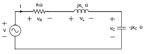
Here, the passive elements such as resistor, inductor and capacitor are connected in series. This entire combination is in series with the input sinusoidal voltage source.
Apply KVL around the loop.
$$V - V_R - V_L - V_C = 0$$
$$\Rightarrow V - IR - I(j X_L) - I(-j X_C) = 0$$
$$\Rightarrow V = IR + I(j X_L) + I(-j X_C)$$
$\Rightarrow V = I[R + j(X_L - X_C)]$Equation 1
The above equation is in the form of V = IZ.
Therefore, the impedance Z of series RLC circuit will be
$$Z = R + j(X_L - X_C)$$
Parameters & Electrical Quantities at Resonance
Now, let us derive the values of parameters and electrical quantities at resonance of series RLC circuit one by one.
Resonant Frequency
The frequency at which resonance occurs is called as resonant frequency fr. In series RLC circuit resonance occurs, when the imaginary term of impedance Z is zero, i.e., the value of $X_L - X_C$ should be equal to zero.
$$\Rightarrow X_L = X_C$$
Substitute $X_L = 2 \pi f L$ and $X_C = \frac{1}{2 \pi f C}$ in the above equation.
$$2 \pi f L = \frac{1}{2 \pi f C}$$
$$\Rightarrow f^2 = \frac{1}{(2 \pi)^2 L C}$$
$$\Rightarrow f = \frac{1}{(2 \pi) \sqrt{LC}}$$
Therefore, the resonant frequency fr of series RLC circuit is
$$f_r = \frac{1}{(2 \pi) \sqrt{LC}}$$
Where, L is the inductance of an inductor and C is the capacitance of a capacitor.
The resonant frequency fr of series RLC circuit depends only on the inductance L and capacitance C. But, it is independent of resistance R.
Impedance
We got the impedance Z of series RLC circuit as
$$Z = R + j(X_L - X_C)$$
Substitute $X_L = X_C$ in the above equation.
$$Z = R + j(X_C - X_C)$$
$$\Rightarrow Z = R + j(0)$$
$$\Rightarrow Z = R$$
At resonance, the impedance Z of series RLC circuit is equal to the value of resistance R, i.e., Z = R.
Current flowing through the Circuit
Substitute $X_L - X_C = 0$ in Equation 1.
$$V = I[R + j(0)]$$
$$\Rightarrow V = IR$$
$$\Rightarrow I = \frac{V}{R}$$
Therefore, current flowing through series RLC circuit at resonance is $\mathbf{\mathit{I = \frac{V}{R}}}$.
At resonance, the impedance of series RLC circuit reaches to minimum value. Hence, the maximum current flows through this circuit at resonance.
Voltage across Resistor
The voltage across resistor is
$$V_R = IR$$
Substitute the value of I in the above equation.
$$V_R = \lgroup \frac{V}{R} \rgroup R$$
$$\Rightarrow V_R = V$$
Therefore, the voltage across resistor at resonance is VR = V.
Voltage across Inductor
The voltage across inductor is
$$V_L = I(jX_L)$$
Substitute the value of I in the above equation.
$$V_L = \lgroup \frac{V}{R} \rgroup (jX_L)$$
$$\Rightarrow V_L = j \lgroup \frac{X_L}{R} \rgroup V$$
$$\Rightarrow V_L = j QV$$
Therefore, the voltage across inductor at resonance is $V_L = j QV$.
So, the magnitude of voltage across inductor at resonance will be
$$|V_L| = QV$$
Where Q is the Quality factor and its value is equal to $\frac{X_L}{R}$
Voltage across Capacitor
The voltage across capacitor is
$$V_C = I(-j X_C)$$
Substitute the value of I in the above equation.
$$V_C = \lgroup \frac{V}{R} \rgroup (-j X_C)$$
$$\Rightarrow V_C = -j \lgroup \frac{X_C}{R} \rgroup V$$
$$\Rightarrow V_C = -jQV$$
Therefore, the voltage across capacitor at resonance is $\mathbf{\mathit{V_C = -jQV}}$.
So, the magnitude of voltage across capacitor at resonance will be
$$|V_C| = QV$$
Where Q is the Quality factor and its value is equal to $\frac{X_{C}}{R}$
Note − Series resonance RLC circuit is called as voltage magnification circuit, because the magnitude of voltage across the inductor and the capacitor is equal to Q times the input sinusoidal voltage V.
Network Theory - Parallel Resonance
In the previous chapter, we discussed the importance of series resonance. Now, let us discuss parallel resonance in RLC circuits.
Parallel Resonance Circuit Diagram
If the resonance occurs in parallel RLC circuit, then it is called as Parallel Resonance. Consider the following parallel RLC circuit, which is represented in phasor domain.
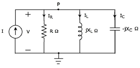
Here, the passive elements such as resistor, inductor and capacitor are connected in parallel. This entire combination is in parallel with the input sinusoidal current source.
Write nodal equation at node P.
$$- I + I_R + I_L + I_C = 0$$
$$\Rightarrow - I + \frac{V}{R} + \frac{V}{j X_L} + \frac{V}{-j X_C} = 0$$
$$\Rightarrow I = \frac{V}{R} - \frac{jV}{X_L} + \frac{jV}{X_C}$$
$\Rightarrow I = V[\frac{1}{R} + j \lgroup \frac{1}{X_C} - \frac{1}{X_L} \rgroup]$Equation 1
The above equation is in the form of I = VY.
Therefore, the admittance Y of parallel RLC circuit will be
$$Y = \frac{1}{R} + j \lgroup \frac{1}{X_C} - \frac{1}{X_L} \rgroup$$
Parameters & Electrical Quantities at Resonance
Now, let us derive the values of parameters and electrical quantities at resonance of parallel RLC circuit one by one.
Resonant Frequency
We know that the resonant frequency, fr is the frequency at which, resonance occurs. In parallel RLC circuit resonance occurs, when the imaginary term of admittance, Y is zero. i.e., the value of $\frac{1}{X_C} - \frac{1}{X_L}$ should be equal to zero
$$\Rightarrow \frac{1}{X_C} = \frac{1}{X_L}$$
$$\Rightarrow X_L = X_C$$
The above resonance condition is same as that of series RLC circuit. So, the resonant frequency, fr will be same in both series RLC circuit and parallel RLC circuit.
Therefore, the resonant frequency, fr of parallel RLC circuit is
$$f_r = \frac{1}{2 \pi \sqrt{LC}}$$
Where,
- L is the inductance of an inductor.
- C is the capacitance of a capacitor.
The resonant frequency, fr of parallel RLC circuit depends only on the inductance L and capacitance C. But, it is independent of resistance R.
Admittance
We got the admittance Y of parallel RLC circuit as
$$Y = \frac{1}{R} + j \lgroup \frac{1}{X_C} - \frac{1}{X_L} \rgroup$$
Substitute, $X_L = X_C$ in the above equation.
$$Y = \frac{1}{R} + j \lgroup \frac{1}{X_C} - \frac{1}{X_C} \rgroup$$
$$\Rightarrow Y = \frac{1}{R} + j(0)$$
$$\Rightarrow Y = \frac{1}{R}$$
At resonance, the admittance, Y of parallel RLC circuit is equal to the reciprocal of the resistance, R. i.e., $\mathbf{\mathit{Y = \frac{1}{R}}}$
Voltage across each Element
Substitute, $\frac{1}{X_C} - \frac{1}{X_L} = 0$ in Equation 1
$$I = V [\frac{1}{R} + j(0)]$$
$$\Rightarrow I = \frac{V}{R}$$
$$\Rightarrow V = IR$$
Therefore, the voltage across all the elements of parallel RLC circuit at resonance is V = IR.
At resonance, the admittance of parallel RLC circuit reaches to minimum value. Hence, maximum voltage is present across each element of this circuit at resonance.
Current flowing through Resistor
The current flowing through resistor is
$$I_R = \frac{V}{R}$$
Substitute the value of V in the above equation.
$$I_R = \frac{IR}{R}$$
$$\Rightarrow I_R = I$$
Therefore, the current flowing through resistor at resonance is $\mathbf{\mathit{I_R = I}}$.
Current flowing through Inductor
The current flowing through inductor is
$$I_L = \frac{V}{j X_L}$$
Substitute the value of V in the above equation.
$$I_L = \frac{IR}{j X_L}$$
$$\Rightarrow I_L = -j \lgroup \frac{R}{X_L} \rgroup I$$
$$\Rightarrow I_L = -jQI$$
Therefore, the current flowing through inductor at resonance is $I_L = -jQI$.
So, the magnitude of current flowing through inductor at resonance will be
$$|I_L| = QI$$
Where, Q is the Quality factor and its value is equal to $\frac{R}{X_L}$
Current flowing through Capacitor
The current flowing through capacitor is
$$I_C = \frac{V}{-j X_C}$$
Substitute the value of V in the above equation.
$$I_C = \frac{IR}{-j X_C}$$
$$\Rightarrow I_C = j \lgroup \frac{R}{X_C} \rgroup I$$
$$\Rightarrow I_C = jQI$$
Therefore, the current flowing through capacitor at resonance is $I_C = jQI$
So, the magnitude of current flowing through capacitor at resonance will be
$$|I_C| = QI$$
Where, Q is the Quality factor and its value is equal to $\frac{R}{X_C}$
Note − Parallel resonance RLC circuit is called as current magnification circuit. Because, the magnitude of current flowing through inductor and capacitor is equal to Q times the input sinusoidal current I.
Network Theory - Coupled Circuits
An electric circuit is said to be a coupled circuit, when there exists a mutual inductance between the coils (or inductors) present in that circuit. Coil is nothing but the series combination of resistor and inductor. In the absence of resistor, coil becomes inductor. Sometimes, the terms coil and inductor are interchangeably used.
In this chapter, first let us discuss about the dot convention and then will discuss about classification of coupling.
Dot Convention
Dot convention is a technique, which gives the details about voltage polarity at the dotted terminal. This information is useful, while writing KVL equations.
If the current enters at the dotted terminal of one coil (or inductor), then it induces a voltage at another coil (or inductor), which is having positive polarity at the dotted terminal.
If the current leaves from the dotted terminal of one coil (or inductor), then it induces a voltage at another coil (or inductor), which is having negative polarity at the dotted terminal.
Classification of Coupling
We can classify coupling into the following two categories.
- Electrical Coupling
- Magnetic Coupling
Now, let us discuss about each type of coupling one by one.
Electrical Coupling
Electrical coupling occurs, when there exists a physical connection between two coils (or inductors). This coupling can be of either aiding type or opposing type. It is based on whether the current enters at the dotted terminal or leaves from the dotted terminal.
Coupling of Aiding type
Consider the following electric circuit, which is having two inductors that are connected in series.
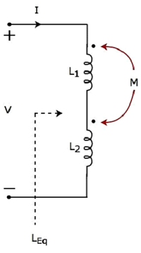
Since the two inductors are connected in series, the same current I flow through both inductors having self-inductances L1 and L2.
In this case, the current, I enter at the dotted terminal of each inductor. Hence, the induced voltage in each inductor will be having positive polarity at the dotted terminal due to the current flowing in another coil.
Apply KVL around the loop of the above electric circuit or network.
$$V - L_1 \frac{dI}{dt} - M \frac{dI}{dt} - L_2 \frac{dI}{dt} - M \frac{dI}{dt} = 0$$
$$V = L_1 \frac{dI}{dt} + L_2 \frac{dI}{dt} + 2M \frac{dI}{dt}$$
$$V = (L_1 + L_2 + 2M)\frac{dI}{dt}$$
The above equation is in the form of $\mathbf{\mathit{V = L_{Eq} \frac{dI}{dt}}}$
Therefore, the equivalent inductance of series combination of inductors shown in the above figure is
$$L_{Eq} = L_1 + L_2 + 2M$$
In this case, the equivalent inductance has been increased by 2M. Hence, the above electrical circuit is an example of electrical coupling which is of aiding type.
Coupling of Opposing type
Consider the following electric circuit, which is having two inductors that are connected in series.
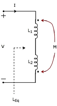
In the above circuit, the current I enters at the dotted terminal of the inductor having an inductance of L1. Hence, it induces a voltage in the other inductor having an inductance of L2. So, positive polarity of the induced voltage is present at the dotted terminal of this inductor.
In the above circuit, the current I leaves from the dotted terminal of the inductor having an inductance of L2. Hence, it induces a voltage in the other inductor having an inductance of L1. So, negative polarity of the induced voltage is present at the dotted terminal of this inductor.
Apply KVL around the loop of the above electric circuit or network.
$$V - L_1 \frac{dI}{dt} + M \frac{dI}{dt} - L_2 \frac{dI}{dt} + M \frac{dI}{dt} = 0$$
$$\Rightarrow V = L_1 \frac{dI}{dt} + L_2 \frac{dI}{dt} - 2M \frac{dI}{dt}$$
$$\Rightarrow V = (L_1 + L_2 - 2M)\frac{dI}{dt}$$
The above equation is in the form of $\mathbf{\mathit{V = L_{Eq} \frac{dI}{dt}}}$
Therefore, the equivalent inductance of series combination of inductors shown in the above figure is
$$L_{Eq} = L_1 + L_2 - 2M$$
In this case, the equivalent inductance has been decreased by 2M. Hence, the above electrical circuit is an example of electrical coupling which is of opposing type.
Magnetic Coupling
Magnetic coupling occurs, when there is no physical connection between two coils (or inductors). This coupling can be of either aiding type or opposing type. It is based on whether the current enters at the dotted terminal or leaves from the dotted terminal.
Coupling of Aiding type
Consider the following electrical equivalent circuit of transformer. It is having two coils and these are called as primary and secondary coils.
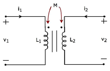
The currents flowing through primary and secondary coils are i1 and i2 respectively. In this case, these currents enter at the dotted terminal of respective coil. Hence, the induced voltage in each coil will be having positive polarity at the dotted terminal due to the current flowing in another coil.
Apply KVL around primary coil.
$$v_1 - L_1 \frac{d i_1}{dt} - M \frac{d i_2}{dt} = 0$$
$\Rightarrow v_1 = L_1 \frac{d i_1}{dt} + M \frac{d i_2}{dt}$Equation 1
Apply KVL around secondary coil.
$$v_2 - L_2 \frac{d i_2}{dt} - M \frac{d i_1}{dt} = 0$$
$\Rightarrow v_2 = L_2 \frac{d i_2}{dt} + M \frac{d i_1}{dt}$Equation 2
In Equation 1 and Equation 2, the self-induced voltage and mutually induced voltage have the same polarity. Hence, the above transformer circuit is an example of magnetic coupling, which is of aiding type.
Coupling of Opposing Type
Consider the following electrical equivalent circuit of transformer.
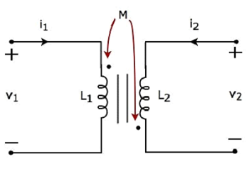
The currents flowing through primary and secondary coils are i1 and i2 respectively. In this case, the current, i1 enters at the dotted terminal of primary coil. Hence, it induces a voltage in secondary coil. So, positive polarity of the induced voltage is present at the dotted terminal of this secondary coil.
In the above circuit, the current, i2 leaves from the dotted terminal of secondary coil. Hence, it induces a voltage in primary coil. So, negative polarity of the induced voltage is present at the dotted terminal of this primary coil.
Apply KVL around primary coil.
$$v_1 - L_1 \frac{d i_1}{dt} + M \frac{d i_2}{dt} = 0$$
$\Rightarrow v_1 = L_1 \frac{d i_1}{dt} - M \frac{d i_2}{dt}$Equation 3
Apply KVL around secondary coil.
$$v_2 - L_2 \frac{d i_2}{dt} + M \frac{d i_1}{dt} = 0$$
$\Rightarrow v_2 = L_2 \frac{d i_2}{dt} - M \frac{d i_1}{dt}$Equation 4
In Equation 3 and Equation 4, self-induced voltage and mutually induced voltage are having opposite polarity. Hence, the above transformer circuit is an example of magnetic coupling, which is of opposing type.
Network Theory - Two-Port Networks
In general, it is easy to analyze any electrical network, if it is represented with an equivalent model, which gives the relation between input and output variables. For this, we can use two port network representations. As the name suggests, two port networks contain two ports. Among which, one port is used as an input port and the other port is used as an output port. The first and second ports are called as port1 and port2 respectively.
One port network is a two terminal electrical network in which, current enters through one terminal and leaves through another terminal. Resistors, inductors and capacitors are the examples of one port network because each one has two terminals. One port network representation is shown in the following figure.
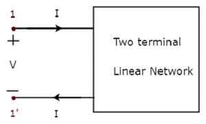
Here, the pair of terminals, 1 & 1’ represents a port. In this case, we are having only one port since it is a one port network.
Similarly, two port network is a pair of two terminal electrical network in which, current enters through one terminal and leaves through another terminal of each port. Two port network representation is shown in the following figure.
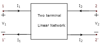
Here, one pair of terminals, 1 & 1’ represents one port, which is called as port1 and the other pair of terminals, 2 & 2’ represents another port, which is called as port2.
There are four variables V1, V2, I1 and I2 in a two port network as shown in the figure. Out of which, we can choose two variables as independent and another two variables as dependent. So, we will get six possible pairs of equations. These equations represent the dependent variables in terms of independent variables. The coefficients of independent variables are called as parameters. So, each pair of equations will give a set of four parameters.
Two Port Network Parameters
The parameters of a two port network are called as two port network parameters or simply, two port parameters. Following are the types of two port network parameters.
- Z parameters
- Y parameters
- T parameters
- T’ parameters
- h-parameters
- g-parameters
Now, let us discuss about these two port network parameters one by one.
Z parameters
We will get the following set of two equations by considering the variables V1 & V2 as dependent and I1 & I2 as independent. The coefficients of independent variables, I1 and I2 are called as Z parameters.
$$V_1 = Z_{11} I_1 + Z_{12} I_2$$
$$V_2 = Z_{21} I_1 + Z_{22} I_2$$
The Z parameters are
$$Z_{11} = \frac{V_1}{I_1}, \: when \: I_2 = 0$$
$$Z_{12} = \frac{V_1}{I_2}, \: when \: I_1 = 0$$
$$Z_{21} = \frac{V_2}{I_1}, \: when \: I_2 = 0$$
$$Z_{22} = \frac{V_2}{I_2}, \: when \: I_1 = 0$$
Z parameters are called as impedance parameters because these are simply the ratios of voltages and currents. Units of Z parameters are Ohm (Ω).
We can calculate two Z parameters, Z11 and Z21, by doing open circuit of port2. Similarly, we can calculate the other two Z parameters, Z12 and Z22 by doing open circuit of port1. Hence, the Z parameters are also called as open-circuit impedance parameters.
Y parameters
We will get the following set of two equations by considering the variables I1 & I2 as dependent and V1 & V2 as independent. The coefficients of independent variables, V1 and V2 are called as Y parameters.
$$I_1 = Y_{11} V_1 + Y_{12} V_2$$
$$I_2 = Y_{21} V_1 + Y_{22} V_2$$
The Y parameters are
$$Y_{11} = \frac{I_1}{V_1}, \: when \: V_2 = 0$$
$$Y_{12} = \frac{I_1}{V_2}, \: when \: V_1 = 0$$
$$Y_{21} = \frac{I_2}{V_1}, \: when \: V_2 = 0$$
$$Y_{22} = \frac{I_2}{V_2}, \: when \: V_1 = 0$$
Y parameters are called as admittance parameters because these are simply, the ratios of currents and voltages. Units of Y parameters are mho.
We can calculate two Y parameters, Y11 and Y21 by doing short circuit of port2. Similarly, we can calculate the other two Y parameters, Y12 and Y22 by doing short circuit of port1. Hence, the Y parameters are also called as short-circuit admittance parameters.
T parameters
We will get the following set of two equations by considering the variables V1 & I1 as dependent and V2 & I2 as independent. The coefficients of V2 and -I2 are called as T parameters.
$$V_1 = A V_2 - B I_2$$
$$I_1 = C V_2 - D I_2$$
The T parameters are
$$A = \frac{V_1}{V_2}, \: when \: I_2 = 0$$
$$B = -\frac{V_1}{I_2}, \: when \: V_2 = 0$$
$$C = \frac{I_1}{V_2}, \: when \: I_2 = 0$$
$$D = -\frac{I_1}{I_2}, \: when \: V_2 = 0$$
T parameters are called as transmission parameters or ABCD parameters. The parameters, A and D do not have any units, since those are dimension less. The units of parameters, B and C are ohm and mho respectively.
We can calculate two parameters, A and C by doing open circuit of port2. Similarly, we can calculate the other two parameters, B and D by doing short circuit of port2.
T ’ parameters
We will get the following set of two equations by considering the variables V2 & I2 as dependent and V1 & I1 as independent. The coefficients of V1 and -I1 are called as T’ parameters.
$$V_2 = A' V_1 - B' I_1$$
$$I_2 = C' V_1 - D' I_1$$
The T’ parameters are
$$A' = \frac{V_2}{V_1}, \: when\: I_1 = 0$$
$$B' = -\frac{V_2}{I_1}, \: when\: V_1 = 0$$
$$C' = \frac{I_2}{V_1}, \: when\: I_1 = 0$$
$$D' = -\frac{I_2}{I_1}, \: when \: V_1 = 0$$
T’ parameters are called as inverse transmission parameters or A’B’C’D’ parameters. The parameters A’ and D’ do not have any units, since those are dimension less. The units of parameters, B’ and C’, are Ohm and Mho respectively.
We can calculate two parameters, A’ and C’, by doing an open circuit of port1. Similarly, we can calculate the other two parameters, B’ and D’, by doing a short circuit of port1.
h-parameters
We will get the following set of two equations by considering the variables V1 & I2 as dependent and I1 & V2 as independent. The coefficients of independent variables, I1 and V2, are called as h-parameters.
$$V_1 = h_{11} I_1 + h_{12} V_2$$
$$I_2 = h_{21} I_1 + h_{22} V_2$$
The h-parameters are
$$h_{11} = \frac{V_1}{I_1},\: when\: V_2 = 0$$
$$h_{12} = \frac{V_1}{V_2},\: when\: I_1 = 0$$
$$h_{21} = \frac{I_2}{I_1},\: when\: V_2 = 0$$
$$h_{22} = \frac{I_2}{V_2},\: when\: I_1 = 0$$
h-parameters are called as hybrid parameters. The parameters, h12 and h21, do not have any units, since those are dimension-less. The units of parameters, h11 and h22, are Ohm and Mho respectively.
We can calculate two parameters, h11 and h21 by doing short circuit of port2. Similarly, we can calculate the other two parameters, h12 and h22 by doing open circuit of port1.
The h-parameters or hybrid parameters are useful in transistor modelling circuits (networks).
g-parameters
We will get the following set of two equations by considering the variables I1 & V2 as dependent and V1 & I2 as independent. The coefficients of independent variables, V1 and I2 are called as g-parameters.
$$I_1 = g_{11} V_1 + g_{12} I_2$$
$$V_2 = g_{21} V_1 + g_{22} I_2$$
The g-parameters are
$$g_{11} = \frac{I_1}{V_1},\: when\: I_2 = 0$$
$$g_{12} = \frac{I_1}{I_2},\: when\: V_1 = 0$$
$$g_{21} = \frac{V_2}{V_1},\: when\: I_2 = 0$$
$$g_{22} = \frac{V_2}{I_2},\: when \: V_1 = 0$$
g-parameters are called as inverse hybrid parameters. The parameters, g12 and g21 do not have any units, since those are dimension less. The units of parameters, g11 and g22 are mho and ohm respectively.
We can calculate two parameters, g11 and g21 by doing open circuit of port2. Similarly, we can calculate the other two parameters, g12 and g22 by doing short circuit of port1.
Two-Port Parameter Conversions
In the previous chapter, we discussed about six types of two-port network parameters. Now, let us convert one set of two-port network parameters into other set of two port network parameters. This conversion is known as two port network parameters conversion or simply, two-port parameters conversion.
Sometimes, it is easy to find one set of parameters of a given electrical network easily. In those situations, we can convert these parameters into the required set of parameters instead of calculating these parameters directly with more difficulty.
Now, let us discuss about some of the two port parameter conversions.
Procedure of two port parameter conversions
Follow these steps, while converting one set of two port network parameters into the other set of two port network parameters.
Step 1 − Write the equations of a two port network in terms of desired parameters.
Step 2 − Write the equations of a two port network in terms of given parameters.
Step 3 − Re-arrange the equations of Step2 in such a way that they should be similar to the equations of Step1.
Step 4 − By equating the similar equations of Step1 and Step3, we will get the desired parameters in terms of given parameters. We can represent these parameters in matrix form.
Z parameters to Y parameters
Here, we have to represent Y parameters in terms of Z parameters. So, in this case Y parameters are the desired parameters and Z parameters are the given parameters.
Step 1 − We know that the following set of two equations, which represents a two port network in terms of Y parameters.
$$I_1 = Y_{11} V_1 + Y_{12} V_2$$
$$I_2 = Y_{21} V_1 + Y_{22} V_2$$
We can represent the above two equations in matrix form as
$\begin{bmatrix}I_1 \\I_2 \end{bmatrix} = \begin{bmatrix}Y_{11} & Y_{12} \\Y_{21} & Y_{22} \end{bmatrix} \begin{bmatrix}V_1 \\V_2 \end{bmatrix}$Equation 1
Step 2 − We know that the following set of two equations, which represents a two port network in terms of Z parameters.
$$V_1 = Z_{11} I_1 + Z_{12} I_2$$
$$V_2 = Z_{21} I_1 + Z_{22} I_2$$
We can represent the above two equations in matrix form as
$$\begin{bmatrix}V_1 \\V_2 \end{bmatrix} = \begin{bmatrix}Z_{11} & Z_{12} \\Z_{21} & Z_{22} \end{bmatrix} \begin{bmatrix}I_1 \\I_2 \end{bmatrix}$$
Step 3 − We can modify it as
$\begin{bmatrix}I_1 \\I_2 \end{bmatrix} = \begin{bmatrix}Z_{11} & Z_{12} \\Z_{21} & Z_{22} \end{bmatrix}^{-1} \begin{bmatrix}V_1 \\V_2 \end{bmatrix}$Equation 2
Step 4 − By equating Equation 1 and Equation 2, we will get
$$\begin{bmatrix}Y_{11} & Y_{12} \\Y_{21} & Y_{22} \end{bmatrix} = \begin{bmatrix}Z_{11} & Z_{12} \\Z_{21} & Z_{22} \end{bmatrix}^{-1} $$
$$\Rightarrow \begin{bmatrix}Y_{11} & Y_{12} \\Y_{21} & Y_{22} \end{bmatrix} = \frac{\begin{bmatrix}Z_{22} & -Z_{12} \\-Z_{21} & Z_{11} \end{bmatrix}}{\Delta Z}$$
Where,
$$\Delta Z = Z_{11} Z_{22} - Z_{12} Z_{21}$$
So, just by doing the inverse of Z parameters matrix, we will get Y parameters matrix.
Z parameters to T parameters
Here, we have to represent T parameters in terms of Z parameters. So, in this case T parameters are the desired parameters and Z parameters are the given parameters.
Step 1 − We know that, the following set of two equations, which represents a two port network in terms of T parameters.
$$V_1 = A V_2 - B I_2$$
$$I_1 = C V_2 - D I_2$$
Step 2 − We know that the following set of two equations, which represents a two port network in terms of Z parameters.
$$V_1 = Z_{11} I_1 + Z_{12} I_2$$
$$V_2 = Z_{21} I_1 + Z_{22} I_2$$
Step 3 − We can modify the above equation as
$$\Rightarrow V_2 - Z_{22} I_2 = Z_{21} I_1$$
$$\Rightarrow I_1 = \lgroup \frac{1}{Z_{21}} \rgroup V_2 - \lgroup \frac{Z_{22}}{Z_{21}} \rgroup I_2$$
Step 4 − The above equation is in the form of $I_1 = CV_2 − DI_2$. Here,
$$C = \frac{1}{Z_{21}}$$
$$D = \frac{Z_{22}}{Z_{21}}$$
Step 5 − Substitute $I_1$ value of Step 3 in $V_1$ equation of Step 2.
$$V_1 = Z_{11} \lbrace \lgroup \frac {1}{Z_{12}} \rgroup V_2 - \lgroup \frac {Z_{22}}{Z_{21}} \rgroup I_2 \rbrace + Z_{12} I_2$$
$$\Rightarrow V_1 = \lgroup \frac {Z_{11}}{Z_{21}} \rgroup V_2 - \lgroup \frac{Z_{11} Z_{22} - Z_{12} Z_{21}}{Z_{21}} \rgroup I_2$$
Step 6 − The above equation is in the form of $V_1 = AV_2 − BI_2$. Here,
$$A = \frac{Z_{11}}{Z_{21}}$$
$$B = \frac{Z_{11} Z_{22} - Z_{12} Z_{21}}{Z_{21}}$$
Step 7 − Therefore, the T parameters matrix is
$$\begin{bmatrix}A & B \\C & D \end{bmatrix} = \begin{bmatrix}\frac{Z_{11}}{Z_{21}} & \frac{Z_{11}Z_{22} - Z_{12}Z_{21}}{Z_{21}} \\\frac{1}{Z_{21}} & \frac{Z_{22}}{Z_{21}} \end{bmatrix}$$
Y parameters to Z parameters
Here, we have to represent Z parameters in terms of Y parameters. So, in this case Z parameters are the desired parameters and Y parameters are the given parameters.
Step 1 − We know that, the following matrix equation of two port network regarding Z parameters as
$\begin{bmatrix}V_1 \\V_2 \end{bmatrix} = \begin{bmatrix}Z_{11} & Z_{12} \\Z_{21} & Z_{22} \end{bmatrix} \begin{bmatrix}I_1 \\I_2 \end{bmatrix}$Equation 3
Step 2 − We know that, the following matrix equation of two port network regarding Y parameters as
$$\begin{bmatrix}I_1 \\I_2 \end{bmatrix} = \begin{bmatrix}Y_{11} & Y_{12} \\Y_{21} & Y_{22} \end{bmatrix} \begin{bmatrix}V_1 \\V_2 \end{bmatrix}$$
Step 3 − We can modify it as
$\begin{bmatrix}V_1 \\V_2 \end{bmatrix} = \begin{bmatrix}Y_{11} & Y_{12} \\Y_{21} & Y_{22} \end{bmatrix}^{-1} \begin{bmatrix}I_1 \\I_2 \end{bmatrix}$Equation 4
Step 4 − By equating Equation 3 and Equation 4, we will get
$$\begin{bmatrix}Z_{11} & Z_{12} \\Z_{21} & Z_{22} \end{bmatrix} = \begin{bmatrix}Y_{11} & Y_{12} \\Y_{21} & Y_{22} \end{bmatrix}^{-1}$$
$$\Rightarrow \begin{bmatrix}Z_{11} & Z_{12} \\Z_{21} & Z_{22} \end{bmatrix} = \frac{\begin{bmatrix}Y_{22} & - Y_{12} \\- Y_{21} & Y_{11} \end{bmatrix}}{\Delta Y}$$
Where,
$$\Delta Y = Y_{11} Y_{22} - Y_{12} Y_{21}$$
So, just by doing the inverse of Y parameters matrix, we will get the Z parameters matrix.
Y parameters to T parameters
Here, we have to represent T parameters in terms of Y parameters. So, in this case, T parameters are the desired parameters and Y parameters are the given parameters.
Step 1 − We know that, the following set of two equations, which represents a two port network in terms of T parameters.
$$V_1 = A V_2 - B I_2$$
$$I_1 = C V_2 - D I_2$$
Step 2 − We know that the following set of two equations of two port network regarding Y parameters.
$$I_1 = Y_{11} V_1 + Y_{12} V_2$$
$$I_2 = Y_{21} V_1 + Y_{22} V_2$$
Step 3 − We can modify the above equation as
$$\Rightarrow I_2 - Y_{22} V_2 = Y_{21} V_1$$
$$\Rightarrow V_1 = \lgroup \frac{- Y_{22}}{Y_{21}} \rgroup V_2 - \lgroup \frac{-1}{Y_{21}} \rgroup I_2$$
Step 4 − The above equation is in the form of $V_1 = AV_2 − BI_2$. Here,
$$A = \frac{- Y_{22}}{Y_{21}}$$
$$B = \frac{-1}{Y_{21}}$$
Step 5 − Substitute $V_1$ value of Step 3 in $I_1$ equation of Step 2.
$$I_1 = Y_{11} \lbrace \lgroup \frac{- Y_{22}}{Y_{21}} \rgroup V_2 - \lgroup \frac{-1}{Y_{21}} \rgroup I_2 \rbrace + Y_{12} V_2$$
$$\Rightarrow I_1 = \lgroup \frac {Y_{12} Y_{21} - Y_{11} Y_{22}}{Y_{21}} \rgroup V_2 - \lgroup \frac{- Y_{11}} {Y_{21}} \rgroup I_2$$
Step 6 − The above equation is in the form of $I_1 = CV_2 − DI_2$. Here,
$$C = \frac {Y_{12} Y_{21} - Y_{11} Y_{22}}{Y_{21}}$$
$$D = \frac{- Y_{11}} {Y_{21}}$$
Step 7 − Therefore, the T parameters matrix is
$$\begin{bmatrix}A & B \\C & D \end{bmatrix} = \begin{bmatrix}\frac{-Y_{22}}{Y_{21}} & \frac{-1}{Y_{21}} \\\frac{Y_{12}Y_{21} - Y_{11}Y_{22}}{Y_{21}} & \frac{-Y_{11}}{Y_{21}} \end{bmatrix}$$
T parameters to h-parameters
Here, we have to represent h-parameters in terms of T parameters. So, in this case hparameters are the desired parameters and T parameters are the given parameters.
Step 1 − We know that, the following h-parameters of a two port network.
$$h_{11} = \frac{V_1}{I_1}, \: when \: V_2 = 0$$
$$h_{12} = \frac{V_1}{V_2}, \: when \: I_1 = 0$$
$$h_{21} = \frac{I_2}{I_1}, \: when \: V_2 = 0$$
$$h_{22} = \frac{I_2}{V_2}, \: when \: I_1 = 0$$
Step 2 − We know that the following set of two equations of two port network regarding T parameters.
$V_1 = A V_2 - B I_2$Equation 5
$I_1 = C V_2 - D I_2$Equation 6
Step 3 − Substitute $V_2 = 0$ in the above equations in order to find the two h-parameters, $h_{11}$ and $h_{21}$.
$$\Rightarrow V_1 = -B I_2$$
$$\Rightarrow I_1 = -D I_2$$
Substitute, $V_1$ and $I_1$ values in h-parameter, $h_{11}$.
$$h_{11} = \frac{-B I_2}{-D I_2}$$
$$\Rightarrow h_{11} = \frac{B}{D}$$
Substitute $I_1$ value in h-parameter $h_{21}$.
$$h_{21} = \frac{I_2}{- D I_2}$$
$$\Rightarrow h_{21} = - \frac{1}{D}$$
Step 4 − Substitute $I_1 = 0$ in the second equation of step 2 in order to find the h-parameter $h_{22}$.
$$0 = C V_2 - D I_2$$
$$\Rightarrow C V_2 = D I_2$$
$$\Rightarrow \frac{I_2}{V_2} = \frac{C}{D}$$
$$\Rightarrow h_{22} = \frac{C}{D}$$
Step 5 − Substitute $I_2 = \lgroup \frac{C}{D} \rgroup V_2$ in the first equation of step 2 in order to find the h-parameter, $h_{12}$.
$$V_1 = A V_2 - B \lgroup \frac{C}{D} \rgroup V_2$$
$$\Rightarrow V_1 = \lgroup \frac{AD - BC}{D} \rgroup V_2$$
$$\Rightarrow \frac{V_1}{V_2} = \frac{AD - BC}{D}$$
$$\Rightarrow h_{12} = \frac{AD - BC}{D}$$
Step 6 − Therefore, the h-parameters matrix is
$$\begin{bmatrix}h_{11} & h_{12} \\h_{21} & h_{22} \end{bmatrix} = \begin{bmatrix}\frac{B}{D} & \frac{AD - BC}{D} \\-\frac{1}{D} & \frac{C}{D} \end{bmatrix}$$
h-parameters to Z parameters
Here, we have to represent Z parameters in terms of h-parameters. So, in this case Z parameters are the desired parameters and h-parameters are the given parameters.
Step 1 − We know that, the following set of two equations of two port network regarding Z parameters.
$$V_1 = Z_{11} I_1 + Z_{12} I_2$$
$$V_2 = Z_{21} I_1 + Z_{22} I_2$$
Step 2 − We know that, the following set of two equations of two-port network regarding h-parameters.
$$V_1 = h_{11} I_1 + h_{12} V_2$$
$$I_2 = h_{21} I_1 + h_{22} V_2$$
Step 3 − We can modify the above equation as
$$\Rightarrow I_2 - h_{21} I_1 = h_{22} V_2$$
$$\Rightarrow V_2 = \frac{I_2 - h_{21} I_1}{h_{22}}$$
$$\Rightarrow V_2 = \lgroup \frac{-h_{21}}{h_{22}} \rgroup I_1 + \lgroup \frac{1}{h_{22}} \rgroup I_2$$
The above equation is in the form of $V_2 = Z_{21} I_1 + Z_{22} I_2. Here,$
$$Z_{21} = \frac{-h_{21}}{h_{22}}$$
$$Z_{22} = \frac{1}{h_{22}}$$
Step 4 − Substitute V2 value in first equation of step 2.
$$V_1 = h_{11} I_1 + h_{21} \lbrace \lgroup \frac{-h_{21}}{h_{22}} \rgroup I_1 + \lgroup \frac{1}{h_{22}} \rgroup I_2 \rbrace$$
$$\Rightarrow V_1 = \lgroup \frac{h_{11}h_{22} - h_{12}h_{21}}{h_{22}} \rgroup I_1 + \lgroup \frac{h_{12}}{h_{22}} \rgroup I_2$$
The above equation is in the form of $V_1 = Z_{11}I_1 + Z_{12}I_2$. Here,
$$Z_{11} = \frac{h_{11}h_{22} - h_{12}h_{21}}{h_{22}}$$
$$Z_{12} = \frac{h_{12}}{h_{22}}$$
Step 5 − Therefore, the Z parameters matrix is
$$\begin{bmatrix}Z_{11} & Z_{12} \\Z_{21} & Z_{22} \end{bmatrix} = \begin{bmatrix}\frac{h_{11}h_{22} - h_{12}h_{21}}{h_{22}} & \frac{h_{12}}{h_{22}} \\\frac{-h_{21}}{h_{22}} & \frac{1}{h_{22}} \end{bmatrix}$$
In this way, we can convert one set of parameters into other set of parameters.
Network Theory - Filters
Filters as the name suggests, they filter the frequency components. That means, they allow certain frequency components and / or reject some other frequency components.
In this chapter, let us discuss about the passive filters. Those are the electric circuits or networks having passive elements like resistor, inductor and capacitor.
Types of Filters
Filters are mainly classified into four types based on the band of frequencies that are allowing and / or the band of frequencies that are rejecting. Following are the types of filters.
- Low Pass Filter
- High Pass Filter
- Band Pass Filter
- Band Stop Filter
Low Pass Filter
Low pass filter as the name suggests, it allows (passes) only low frequency components. That means, it rejects (blocks) all other high frequency components.
The s-domain circuit diagram (network) of Low Pass Filter is shown in the following figure.
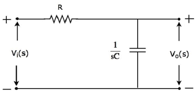
It consists of two passive elements resistor and capacitor, which are connected in series. Input voltage is applied across this entire combination and the output is considered as the voltage across capacitor.
Here, $V_i(s)$ and $V_o(s)$ are the Laplace transforms of input voltage, $v_i(t)$ and output voltage, $v_o(t)$ respectively.
The transfer function of the above network is
$$H(s) = \frac{V_o(s)}{V_i(s)} = \frac{\frac{1}{sC}}{R + \frac{1}{sC}}$$
$$\Rightarrow H(s) = \frac{1}{1 + sCR}$$
Substitute, $s = j \omega$ in the above equation.
$$H(j \omega) = \frac{1}{1 + j \omega CR}$$
Magnitude of transfer function is
$$|H(j \omega)| = \frac{1}{\sqrt{(1 + (\omega CR)^2}}$$
At ω = 0, the magnitude of transfer function is equal to 1.
At $\omega = \frac{1}{CR}$, the magnitude of transfer function is equal to 0.707.
At ω = ∞, the magnitude of transfer function is equal to 0.
Therefore, the magnitude of transfer function of Low pass filter will vary from 1 to 0 as ω varies from 0 to ∞.
High Pass Filter
High pass filter as the name suggests, it allows (passes) only high frequency components. That means, it rejects (blocks) all low frequency components.
The s-domain circuit diagram (network) of High pass filter is shown in the following figure.
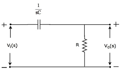
It consists of two passive elements capacitor and resistor, which are connected in series. Input voltage is applied across this entire combination and the output is considered as the voltage across resistor.
Here, $V_i(s)$ and $V_o(s)$ are the Laplace transforms of input voltage, $v_i(t)$ and output voltage, $v_o(t)$ respectively.
The transfer function of the above network is
$$H(s) = \frac{V_o(s)}{V_i(s)} = \frac{R}{R + \frac{1}{sC}}$$
$$\Rightarrow H(s) = \frac{sCR}{1 + sCR}$$
Substitute, $s = j \omega$ in the above equation.
$$H(j \omega) = \frac{j \omega CR}{1 + j \omega CR}$$
Magnitude of transfer function is
$$|H(j \omega)| = \frac{\omega CR}{\sqrt{(1 + (\omega CR)^2}}$$
At ω = 0, the magnitude of transfer function is equal to 0.
At $\omega = \frac{1}{CR}$, the magnitude of transfer function is equal to 0.707.
At ω = ∞, the magnitude of transfer function is equal to 1.
Therefore, the magnitude of transfer function of High pass filter will vary from 0 to 1 as ω varies from 0 to ∞.
Band Pass Filter
Band pass filter as the name suggests, it allows (passes) only one band of frequencies. In general, this frequency band lies in between low frequency range and high frequency range. That means, this filter rejects (blocks) both low and high frequency components.
The s-domain circuit diagram (network) of Band pass filter is shown in the following figure.
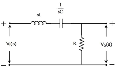
It consists of three passive elements inductor, capacitor and resistor, which are connected in series. Input voltage is applied across this entire combination and the output is considered as the voltage across resistor.
Here, $V_i(s)$ and $V_o(s)$ are the Laplace transforms of input voltage, $v_i(t)$ and output voltage, $v_o(t)$ respectively.
The transfer function of the above network is
$$H(s) = \frac{V_o(s)}{V_i(s)} = \frac{R}{R + \frac{1}{sC} + sL}$$
$$\Rightarrow H(s) = \frac{s CR}{s^2 LC + sCR + 1}$$
Substitute $s = j \omega$ in the above equation.
$$H(j \omega) = \frac{j \omega CR}{1 - \omega^2 LC + j \omega CR}$$
Magnitude of transfer function is
$$|H(j \omega)| = \frac{\omega CR}{\sqrt{(1 - \omega^2 LC)^2 + (\omega CR)^2}}$$
At ω = 0, the magnitude of transfer function is equal to 0.
At $\omega = \frac{1}{\sqrt{LC}}$, the magnitude of transfer function is equal to 1.
At ω = ∞, the magnitude of transfer function is equal to 0.
Therefore, the magnitude of transfer function of Band pass filter will vary from 0 to 1 & 1 to 0 as ω varies from 0 to ∞.
Band Stop Filter
Band stop filter as the name suggests, it rejects (blocks) only one band of frequencies. In general, this frequency band lies in between low frequency range and high frequency range. That means, this filter allows (passes) both low and high frequency components.
The s-domain (network) of circuit diagramand stop filter is shown in the following figure.
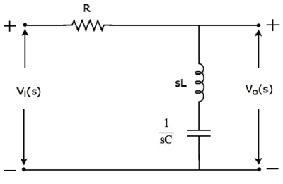
It consists of three passive elements resistor, inductor and capacitor, which are connected in series. Input voltage is applied across this entire combination and the output is considered as the voltage across the combination of inductor and capacitor.
Here, $V_i(s)$ and $V_o(s)$ are the Laplace transforms of input voltage, $v_i(t)$ and output voltage, $v_o(t)$ respectively.
The transfer function of the above network is
$$H(s) = \frac{V_o(s)}{V_i(s)} = \frac{sL + \frac{1}{sC}}{R + sL + \frac{1}{sC}}$$
$$\Rightarrow H(s) = \frac{s^2 LC + 1}{s^2 LC + sCR + 1}$$
Substitute, $s = j \omega$ in the above equation.
$$H(j \omega) = \frac{1 - \omega^2 LC}{1 - \omega^2 LC + j \omega CR}$$
Magnitude of transfer function is
$$|H(j \omega)| = \frac{1 - \omega^2 LC}{\sqrt{(1 - \omega^2 LC)^2 + (\omega CR)^2}}$$
At ω = 0, the magnitude of transfer function is equal to 1.
At $\omega = \frac{1}{\sqrt{LC}}$, the magnitude of transfer function is equal to 0.
At ω = ∞, the magnitude of transfer function is equal to 1.
Therefore, the magnitude of transfer function of Band stop filter will vary from 1 to 0 & 0 to 1 as ω varies from 0 to ∞.