
- Microprocessor Tutorial
- Microprocessor - Home
- Microprocessor - Overview
- Microprocessor - Classification
- 8085 Microprocessor
- Microprocessor - 8085 Architecture
- 8085 Pin Configuration
- Addressing Modes & Interrupts
- 8085 Instruction Sets
- 8086 Microprocessor
- Microprocessor - 8086 Overview
- 8086 Functional Units
- 8086 Pin Configuration
- 8086 Instruction Sets
- Microprocessor - 8086 Interrupts
- 8086 Addressing Modes
- Multiprocessor Configuration
- Configuration Overview
- 8087 Numeric Data Processor
- I/O Interfacing
- I/O Interfacing Overview
- 8279 Programmable Keyboard
- 8257 DMA Controller
- Microcontrollers
- Microcontrollers - Overview
- Microcontrollers - 8051 Architecture
- 8051 Pin Description
- 8051 Input Output Ports
- Microcontrollers - 8051 Interrupts
- Peripheral Devices
- Programmable Peripheral Interface
- Intel 8255A - Pin Description
- 8253 - Programmable Interval Timer
- 8253/54 - Operational Modes
- Microprocessor Useful Resources
- Microprocessor - Quick Guide
- Microprocessor - Useful Resources
- Microprocessor - Discussion
Microprocessor - Quick Guide
Microprocessor - Overview
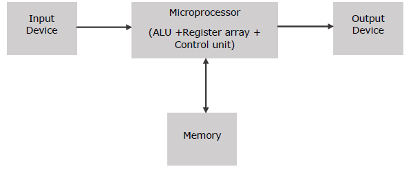
Microprocessor is a controlling unit of a micro-computer, fabricated on a small chip capable of performing ALU (Arithmetic Logical Unit) operations and communicating with the other devices connected to it.
Microprocessor consists of an ALU, register array, and a control unit. ALU performs arithmetical and logical operations on the data received from the memory or an input device. Register array consists of registers identified by letters like B, C, D, E, H, L and accumulator. The control unit controls the flow of data and instructions within the computer.
Block Diagram of a Basic Microcomputer
How does a Microprocessor Work?
The microprocessor follows a sequence: Fetch, Decode, and then Execute.
Initially, the instructions are stored in the memory in a sequential order. The microprocessor fetches those instructions from the memory, then decodes it and executes those instructions till STOP instruction is reached. Later, it sends the result in binary to the output port. Between these processes, the register stores the temporarily data and ALU performs the computing functions.
List of Terms Used in a Microprocessor
Here is a list of some of the frequently used terms in a microprocessor −
Instruction Set − It is the set of instructions that the microprocessor can understand.
Bandwidth − It is the number of bits processed in a single instruction.
Clock Speed − It determines the number of operations per second the processor can perform. It is expressed in megahertz (MHz) or gigahertz (GHz).It is also known as Clock Rate.
Word Length − It depends upon the width of internal data bus, registers, ALU, etc. An 8-bit microprocessor can process 8-bit data at a time. The word length ranges from 4 bits to 64 bits depending upon the type of the microcomputer.
Data Types − The microprocessor has multiple data type formats like binary, BCD, ASCII, signed and unsigned numbers.
Features of a Microprocessor
Here is a list of some of the most prominent features of any microprocessor −
Cost-effective − The microprocessor chips are available at low prices and results its low cost.
Size − The microprocessor is of small size chip, hence is portable.
Low Power Consumption − Microprocessors are manufactured by using metaloxide semiconductor technology, which has low power consumption.
Versatility − The microprocessors are versatile as we can use the same chip in a number of applications by configuring the software program.
Reliability − The failure rate of an IC in microprocessors is very low, hence it is reliable.
Microprocessor - Classification
A microprocessor can be classified into three categories −
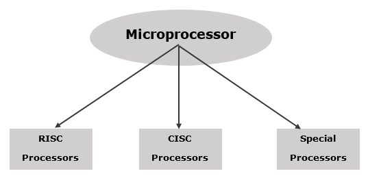
RISC Processor
RISC stands for Reduced Instruction Set Computer. It is designed to reduce the execution time by simplifying the instruction set of the computer. Using RISC processors, each instruction requires only one clock cycle to execute results in uniform execution time. This reduces the efficiency as there are more lines of code, hence more RAM is needed to store the instructions. The compiler also has to work more to convert high-level language instructions into machine code.
Some of the RISC processors are −
- Power PC: 601, 604, 615, 620
- DEC Alpha: 210642, 211066, 21068, 21164
- MIPS: TS (R10000) RISC Processor
- PA-RISC: HP 7100LC
Architecture of RISC
RISC microprocessor architecture uses highly-optimized set of instructions. It is used in portable devices like Apple iPod due to its power efficiency.
Characteristics of RISC
The major characteristics of a RISC processor are as follows −
It consists of simple instructions.
It supports various data-type formats.
It utilizes simple addressing modes and fixed length instructions for pipelining.
It supports register to use in any context.
One cycle execution time.
“LOAD” and “STORE” instructions are used to access the memory location.
It consists of larger number of registers.
It consists of less number of transistors.
CISC Processor
CISC stands for Complex Instruction Set Computer. It is designed to minimize the number of instructions per program, ignoring the number of cycles per instruction. The emphasis is on building complex instructions directly into the hardware.
The compiler has to do very little work to translate a high-level language into assembly level language/machine code because the length of the code is relatively short, so very little RAM is required to store the instructions.
Some of the CISC Processors are −
- IBM 370/168
- VAX 11/780
- Intel 80486
Architecture of CISC
Its architecture is designed to decrease the memory cost because more storage is needed in larger programs resulting in higher memory cost. To resolve this, the number of instructions per program can be reduced by embedding the number of operations in a single instruction.
Characteristics of CISC
- Variety of addressing modes.
- Larger number of instructions.
- Variable length of instruction formats.
- Several cycles may be required to execute one instruction.
- Instruction-decoding logic is complex.
- One instruction is required to support multiple addressing modes.
Special Processors
These are the processors which are designed for some special purposes. Few of the special processors are briefly discussed −
Coprocessor
A coprocessor is a specially designed microprocessor, which can handle its particular function many times faster than the ordinary microprocessor.
For example − Math Coprocessor.
Some Intel math-coprocessors are −
- 8087-used with 8086
- 80287-used with 80286
- 80387-used with 80386
Input/Output Processor
It is a specially designed microprocessor having a local memory of its own, which is used to control I/O devices with minimum CPU involvement.
For example −
- DMA (direct Memory Access) controller
- Keyboard/mouse controller
- Graphic display controller
- SCSI port controller
Transputer (Transistor Computer)
A transputer is a specially designed microprocessor with its own local memory and having links to connect one transputer to another transputer for inter-processor communications. It was first designed in 1980 by Inmos and is targeted to the utilization of VLSI technology.
A transputer can be used as a single processor system or can be connected to external links, which reduces the construction cost and increases the performance.
For example − 16-bit T212, 32-bit T425, the floating point (T800, T805 & T9000) processors.
DSP (Digital Signal Processor)
This processor is specially designed to process the analog signals into a digital form. This is done by sampling the voltage level at regular time intervals and converting the voltage at that instant into a digital form. This process is performed by a circuit called an analogue to digital converter, A to D converter or ADC.
A DSP contains the following components −
Program Memory − It stores the programs that DSP will use to process data.
Data Memory − It stores the information to be processed.
Compute Engine − It performs the mathematical processing, accessing the program from the program memory and the data from the data memory.
Input/Output − It connects to the outside world.
Its applications are −
- Sound and music synthesis
- Audio and video compression
- Video signal processing
- 2D and 3d graphics acceleration.
For example − Texas Instrument’s TMS 320 series, e.g., TMS 320C40, TMS320C50.
Microprocessor - 8085 Architecture
8085 is pronounced as "eighty-eighty-five" microprocessor. It is an 8-bit microprocessor designed by Intel in 1977 using NMOS technology.
It has the following configuration −
- 8-bit data bus
- 16-bit address bus, which can address upto 64KB
- A 16-bit program counter
- A 16-bit stack pointer
- Six 8-bit registers arranged in pairs: BC, DE, HL
- Requires +5V supply to operate at 3.2 MHZ single phase clock
It is used in washing machines, microwave ovens, mobile phones, etc.
8085 Microprocessor – Functional Units
8085 consists of the following functional units −
Accumulator
It is an 8-bit register used to perform arithmetic, logical, I/O & LOAD/STORE operations. It is connected to internal data bus & ALU.
Arithmetic and logic unit
As the name suggests, it performs arithmetic and logical operations like Addition, Subtraction, AND, OR, etc. on 8-bit data.
General purpose register
There are 6 general purpose registers in 8085 processor, i.e. B, C, D, E, H & L. Each register can hold 8-bit data.
These registers can work in pair to hold 16-bit data and their pairing combination is like B-C, D-E & H-L.
Program counter
It is a 16-bit register used to store the memory address location of the next instruction to be executed. Microprocessor increments the program whenever an instruction is being executed, so that the program counter points to the memory address of the next instruction that is going to be executed.
Stack pointer
It is also a 16-bit register works like stack, which is always incremented/decremented by 2 during push & pop operations.
Temporary register
It is an 8-bit register, which holds the temporary data of arithmetic and logical operations.
Flag register
It is an 8-bit register having five 1-bit flip-flops, which holds either 0 or 1 depending upon the result stored in the accumulator.
These are the set of 5 flip-flops −
- Sign (S)
- Zero (Z)
- Auxiliary Carry (AC)
- Parity (P)
- Carry (C)
Its bit position is shown in the following table −
| D7 | D6 | D5 | D4 | D3 | D2 | D1 | D0 |
|---|---|---|---|---|---|---|---|
| S | Z | AC | P | CY |
Instruction register and decoder
It is an 8-bit register. When an instruction is fetched from memory then it is stored in the Instruction register. Instruction decoder decodes the information present in the Instruction register.
Timing and control unit
It provides timing and control signal to the microprocessor to perform operations. Following are the timing and control signals, which control external and internal circuits −
- Control Signals: READY, RD’, WR’, ALE
- Status Signals: S0, S1, IO/M’
- DMA Signals: HOLD, HLDA
- RESET Signals: RESET IN, RESET OUT
Interrupt control
As the name suggests it controls the interrupts during a process. When a microprocessor is executing a main program and whenever an interrupt occurs, the microprocessor shifts the control from the main program to process the incoming request. After the request is completed, the control goes back to the main program.
There are 5 interrupt signals in 8085 microprocessor: INTR, RST 7.5, RST 6.5, RST 5.5, TRAP.
Serial Input/output control
It controls the serial data communication by using these two instructions: SID (Serial input data) and SOD (Serial output data).
Address buffer and address-data buffer
The content stored in the stack pointer and program counter is loaded into the address buffer and address-data buffer to communicate with the CPU. The memory and I/O chips are connected to these buses; the CPU can exchange the desired data with the memory and I/O chips.
Address bus and data bus
Data bus carries the data to be stored. It is bidirectional, whereas address bus carries the location to where it should be stored and it is unidirectional. It is used to transfer the data & Address I/O devices.
8085 Architecture
We have tried to depict the architecture of 8085 with this following image −
Microprocessor - 8085 Pin Configuration
The following image depicts the pin diagram of 8085 Microprocessor −
The pins of a 8085 microprocessor can be classified into seven groups −
Address bus
A15-A8, it carries the most significant 8-bits of memory/IO address.
Data bus
AD7-AD0, it carries the least significant 8-bit address and data bus.
Control and status signals
These signals are used to identify the nature of operation. There are 3 control signal and 3 status signals.
Three control signals are RD, WR & ALE.
RD − This signal indicates that the selected IO or memory device is to be read and is ready for accepting data available on the data bus.
WR − This signal indicates that the data on the data bus is to be written into a selected memory or IO location.
ALE − It is a positive going pulse generated when a new operation is started by the microprocessor. When the pulse goes high, it indicates address. When the pulse goes down it indicates data.
Three status signals are IO/M, S0 & S1.
IO/M
This signal is used to differentiate between IO and Memory operations, i.e. when it is high indicates IO operation and when it is low then it indicates memory operation.
S1 & S0
These signals are used to identify the type of current operation.
Power supply
There are 2 power supply signals − VCC & VSS. VCC indicates +5v power supply and VSS indicates ground signal.
Clock signals
There are 3 clock signals, i.e. X1, X2, CLK OUT.
X1, X2 − A crystal (RC, LC N/W) is connected at these two pins and is used to set frequency of the internal clock generator. This frequency is internally divided by 2.
CLK OUT − This signal is used as the system clock for devices connected with the microprocessor.
Interrupts & externally initiated signals
Interrupts are the signals generated by external devices to request the microprocessor to perform a task. There are 5 interrupt signals, i.e. TRAP, RST 7.5, RST 6.5, RST 5.5, and INTR. We will discuss interrupts in detail in interrupts section.
INTA − It is an interrupt acknowledgment signal.
RESET IN − This signal is used to reset the microprocessor by setting the program counter to zero.
RESET OUT − This signal is used to reset all the connected devices when the microprocessor is reset.
READY − This signal indicates that the device is ready to send or receive data. If READY is low, then the CPU has to wait for READY to go high.
HOLD − This signal indicates that another master is requesting the use of the address and data buses.
HLDA (HOLD Acknowledge) − It indicates that the CPU has received the HOLD request and it will relinquish the bus in the next clock cycle. HLDA is set to low after the HOLD signal is removed.
Serial I/O signals
There are 2 serial signals, i.e. SID and SOD and these signals are used for serial communication.
SOD (Serial output data line) − The output SOD is set/reset as specified by the SIM instruction.
SID (Serial input data line) − The data on this line is loaded into accumulator whenever a RIM instruction is executed.
8085 Addressing Modes & Interrupts
Now let us discuss the addressing modes in 8085 Microprocessor.
Addressing Modes in 8085
These are the instructions used to transfer the data from one register to another register, from the memory to the register, and from the register to the memory without any alteration in the content. Addressing modes in 8085 is classified into 5 groups −
Immediate addressing mode
In this mode, the 8/16-bit data is specified in the instruction itself as one of its operand. For example: MVI K, 20F: means 20F is copied into register K.
Register addressing mode
In this mode, the data is copied from one register to another. For example: MOV K, B: means data in register B is copied to register K.
Direct addressing mode
In this mode, the data is directly copied from the given address to the register. For example: LDB 5000K: means the data at address 5000K is copied to register B.
Indirect addressing mode
In this mode, the data is transferred from one register to another by using the address pointed by the register. For example: MOV K, B: means data is transferred from the memory address pointed by the register to the register K.
Implied addressing mode
This mode doesn’t require any operand; the data is specified by the opcode itself. For example: CMP.
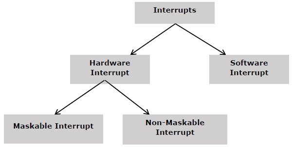
Interrupts in 8085
Interrupts are the signals generated by the external devices to request the microprocessor to perform a task. There are 5 interrupt signals, i.e. TRAP, RST 7.5, RST 6.5, RST 5.5, and INTR.
Interrupt are classified into following groups based on their parameter −
Vector interrupt − In this type of interrupt, the interrupt address is known to the processor. For example: RST7.5, RST6.5, RST5.5, TRAP.
Non-Vector interrupt − In this type of interrupt, the interrupt address is not known to the processor so, the interrupt address needs to be sent externally by the device to perform interrupts. For example: INTR.
Maskable interrupt − In this type of interrupt, we can disable the interrupt by writing some instructions into the program. For example: RST7.5, RST6.5, RST5.5.
Non-Maskable interrupt − In this type of interrupt, we cannot disable the interrupt by writing some instructions into the program. For example: TRAP.
Software interrupt − In this type of interrupt, the programmer has to add the instructions into the program to execute the interrupt. There are 8 software interrupts in 8085, i.e. RST0, RST1, RST2, RST3, RST4, RST5, RST6, and RST7.
Hardware interrupt − There are 5 interrupt pins in 8085 used as hardware interrupts, i.e. TRAP, RST7.5, RST6.5, RST5.5, INTA.
Note − NTA is not an interrupt, it is used by the microprocessor for sending acknowledgement. TRAP has the highest priority, then RST7.5 and so on.
Interrupt Service Routine (ISR)
A small program or a routine that when executed, services the corresponding interrupting source is called an ISR.
TRAP
It is a non-maskable interrupt, having the highest priority among all interrupts. Bydefault, it is enabled until it gets acknowledged. In case of failure, it executes as ISR and sends the data to backup memory. This interrupt transfers the control to the location 0024H.
RST7.5
It is a maskable interrupt, having the second highest priority among all interrupts. When this interrupt is executed, the processor saves the content of the PC register into the stack and branches to 003CH address.
RST 6.5
It is a maskable interrupt, having the third highest priority among all interrupts. When this interrupt is executed, the processor saves the content of the PC register into the stack and branches to 0034H address.
RST 5.5
It is a maskable interrupt. When this interrupt is executed, the processor saves the content of the PC register into the stack and branches to 002CH address.
INTR
It is a maskable interrupt, having the lowest priority among all interrupts. It can be disabled by resetting the microprocessor.
When INTR signal goes high, the following events can occur −
The microprocessor checks the status of INTR signal during the execution of each instruction.
When the INTR signal is high, then the microprocessor completes its current instruction and sends active low interrupt acknowledge signal.
When instructions are received, then the microprocessor saves the address of the next instruction on stack and executes the received instruction.
Microprocessor - 8085 Instruction Sets
Let us take a look at the programming of 8085 Microprocessor.
Instruction sets are instruction codes to perform some task. It is classified into five categories.
| S.No. | Instruction & Description |
|---|---|
| 1 | Control Instructions
Following is the table showing the list of Control instructions with their meanings. |
| 2 | Logical Instructions
Following is the table showing the list of Logical instructions with their meanings. |
| 3 | Branching Instructions
Following is the table showing the list of Branching instructions with their meanings. |
| 4 | Arithmetic Instructions
Following is the table showing the list of Arithmetic instructions with their meanings. |
| 5 | Data Transfer Instructions
Following is the table showing the list of Data-transfer instructions with their meanings. |
8085 – Demo Programs
Now, let us take a look at some program demonstrations using the above instructions −
Adding Two 8-bit Numbers
Write a program to add data at 3005H & 3006H memory location and store the result at 3007H memory location.
Problem demo −
(3005H) = 14H
   (3006H) = 89H
Result −
14H + 89H = 9DH
The program code can be written like this −
LXI H 3005H   : "HL points 3005H"
MOV A, M      : "Getting first operand"
INX H         : "HL points 3006H"
ADD M         : "Add second operand"
INX H         : "HL points 3007H"
MOV M, A      : "Store result at 3007H"
HLT           : "Exit program"
Exchanging the Memory Locations
Write a program to exchange the data at 5000M& 6000M memory location.
LDA 5000M   : "Getting the contents at5000M location into accumulator"
MOV B, A    : "Save the contents into B register"
LDA 6000M   : "Getting the contents at 6000M location into accumulator"
STA 5000M   : "Store the contents of accumulator at address 5000M"
MOV A, B    : "Get the saved contents back into A register"
STA 6000M   : "Store the contents of accumulator at address 6000M"
Arrange Numbers in an Ascending Order
Write a program to arrange first 10 numbers from memory address 3000H in an ascending order.
MVI B, 09         :"Initialize counter"
START             :"LXI H, 3000H: Initialize memory pointer"
MVI C, 09H        :"Initialize counter 2"
BACK: MOV A, M    :"Get the number"
INX H             :"Increment memory pointer"
CMP M             :"Compare number with next number"
JC SKIP           :"If less, don’t interchange"
JZ SKIP           :"If equal, don’t interchange"
MOV D, M
MOV M, A
DCX H
MOV M, D
INX H             :"Interchange two numbers"
SKIP:DCR C        :"Decrement counter 2"
JNZ BACK          :"If not zero, repeat"
DCR B             :"Decrement counter 1"
JNZ START
HLT               :"Terminate program execution"
Microprocessor - 8086 Overview
8086 Microprocessor is an enhanced version of 8085Microprocessor that was designed by Intel in 1976. It is a 16-bit Microprocessor having 20 address lines and16 data lines that provides up to 1MB storage. It consists of powerful instruction set, which provides operations like multiplication and division easily.
It supports two modes of operation, i.e. Maximum mode and Minimum mode. Maximum mode is suitable for system having multiple processors and Minimum mode is suitable for system having a single processor.
Features of 8086
The most prominent features of a 8086 microprocessor are as follows −
It has an instruction queue, which is capable of storing six instruction bytes from the memory resulting in faster processing.
It was the first 16-bit processor having 16-bit ALU, 16-bit registers, internal data bus, and 16-bit external data bus resulting in faster processing.
It is available in 3 versions based on the frequency of operation −
8086 → 5MHz
8086-2 → 8MHz
(c)8086-1 → 10 MHz
It uses two stages of pipelining, i.e. Fetch Stage and Execute Stage, which improves performance.
Fetch stage can prefetch up to 6 bytes of instructions and stores them in the queue.
Execute stage executes these instructions.
It has 256 vectored interrupts.
It consists of 29,000 transistors.
Comparison between 8085 & 8086 Microprocessor
Size − 8085 is 8-bit microprocessor, whereas 8086 is 16-bit microprocessor.
Address Bus − 8085 has 16-bit address bus while 8086 has 20-bit address bus.
Memory − 8085 can access up to 64Kb, whereas 8086 can access up to 1 Mb of memory.
Instruction − 8085 doesn’t have an instruction queue, whereas 8086 has an instruction queue.
Pipelining − 8085 doesn’t support a pipelined architecture while 8086 supports a pipelined architecture.
I/O − 8085 can address 2^8 = 256 I/O's, whereas 8086 can access 2^16 = 65,536 I/O's.
Cost − The cost of 8085 is low whereas that of 8086 is high.
Architecture of 8086
The following diagram depicts the architecture of a 8086 Microprocessor −
Microprocessor - 8086 Functional Units
8086 Microprocessor is divided into two functional units, i.e., EU (Execution Unit) and BIU (Bus Interface Unit).
EU (Execution Unit)
Execution unit gives instructions to BIU stating from where to fetch the data and then decode and execute those instructions. Its function is to control operations on data using the instruction decoder & ALU. EU has no direct connection with system buses as shown in the above figure, it performs operations over data through BIU.
Let us now discuss the functional parts of 8086 microprocessors.
ALU
It handles all arithmetic and logical operations, like +, −, ×, /, OR, AND, NOT operations.
Flag Register
It is a 16-bit register that behaves like a flip-flop, i.e. it changes its status according to the result stored in the accumulator. It has 9 flags and they are divided into 2 groups − Conditional Flags and Control Flags.
Conditional Flags
It represents the result of the last arithmetic or logical instruction executed. Following is the list of conditional flags −
Carry flag − This flag indicates an overflow condition for arithmetic operations.
Auxiliary flag − When an operation is performed at ALU, it results in a carry/barrow from lower nibble (i.e. D0 – D3) to upper nibble (i.e. D4 – D7), then this flag is set, i.e. carry given by D3 bit to D4 is AF flag. The processor uses this flag to perform binary to BCD conversion.
Parity flag − This flag is used to indicate the parity of the result, i.e. when the lower order 8-bits of the result contains even number of 1’s, then the Parity Flag is set. For odd number of 1’s, the Parity Flag is reset.
Zero flag − This flag is set to 1 when the result of arithmetic or logical operation is zero else it is set to 0.
Sign flag − This flag holds the sign of the result, i.e. when the result of the operation is negative, then the sign flag is set to 1 else set to 0.
Overflow flag − This flag represents the result when the system capacity is exceeded.
Control Flags
Control flags controls the operations of the execution unit. Following is the list of control flags −
Trap flag − It is used for single step control and allows the user to execute one instruction at a time for debugging. If it is set, then the program can be run in a single step mode.
Interrupt flag − It is an interrupt enable/disable flag, i.e. used to allow/prohibit the interruption of a program. It is set to 1 for interrupt enabled condition and set to 0 for interrupt disabled condition.
Direction flag − It is used in string operation. As the name suggests when it is set then string bytes are accessed from the higher memory address to the lower memory address and vice-a-versa.
General purpose register
There are 8 general purpose registers, i.e., AH, AL, BH, BL, CH, CL, DH, and DL. These registers can be used individually to store 8-bit data and can be used in pairs to store 16bit data. The valid register pairs are AH and AL, BH and BL, CH and CL, and DH and DL. It is referred to the AX, BX, CX, and DX respectively.
AX register − It is also known as accumulator register. It is used to store operands for arithmetic operations.
BX register − It is used as a base register. It is used to store the starting base address of the memory area within the data segment.
CX register − It is referred to as counter. It is used in loop instruction to store the loop counter.
DX register − This register is used to hold I/O port address for I/O instruction.
Stack pointer register
It is a 16-bit register, which holds the address from the start of the segment to the memory location, where a word was most recently stored on the stack.
BIU (Bus Interface Unit)
BIU takes care of all data and addresses transfers on the buses for the EU like sending addresses, fetching instructions from the memory, reading data from the ports and the memory as well as writing data to the ports and the memory. EU has no direction connection with System Buses so this is possible with the BIU. EU and BIU are connected with the Internal Bus.
It has the following functional parts −
Instruction queue − BIU contains the instruction queue. BIU gets upto 6 bytes of next instructions and stores them in the instruction queue. When EU executes instructions and is ready for its next instruction, then it simply reads the instruction from this instruction queue resulting in increased execution speed.
Fetching the next instruction while the current instruction executes is called pipelining.
Segment register − BIU has 4 segment buses, i.e. CS, DS, SS& ES. It holds the addresses of instructions and data in memory, which are used by the processor to access memory locations. It also contains 1 pointer register IP, which holds the address of the next instruction to executed by the EU.
CS − It stands for Code Segment. It is used for addressing a memory location in the code segment of the memory, where the executable program is stored.
DS − It stands for Data Segment. It consists of data used by the program andis accessed in the data segment by an offset address or the content of other register that holds the offset address.
SS − It stands for Stack Segment. It handles memory to store data and addresses during execution.
ES − It stands for Extra Segment. ES is additional data segment, which is used by the string to hold the extra destination data.
Instruction pointer − It is a 16-bit register used to hold the address of the next instruction to be executed.
Microprocessor - 8086 Pin Configuration
8086 was the first 16-bit microprocessor available in 40-pin DIP (Dual Inline Package) chip. Let us now discuss in detail the pin configuration of a 8086 Microprocessor.
8086 Pin Diagram
Here is the pin diagram of 8086 microprocessor −
Let us now discuss the signals in detail −
Power supply and frequency signals
It uses 5V DC supply at VCC pin 40, and uses ground at VSS pin 1 and 20 for its operation.
Clock signal
Clock signal is provided through Pin-19. It provides timing to the processor for operations. Its frequency is different for different versions, i.e. 5MHz, 8MHz and 10MHz.
Address/data bus
AD0-AD15. These are 16 address/data bus. AD0-AD7 carries low order byte data and AD8AD15 carries higher order byte data. During the first clock cycle, it carries 16-bit address and after that it carries 16-bit data.
Address/status bus
A16-A19/S3-S6. These are the 4 address/status buses. During the first clock cycle, it carries 4-bit address and later it carries status signals.
S7/BHE
BHE stands for Bus High Enable. It is available at pin 34 and used to indicate the transfer of data using data bus D8-D15. This signal is low during the first clock cycle, thereafter it is active.
Read($\overline{RD}$)
It is available at pin 32 and is used to read signal for Read operation.
Ready
It is available at pin 22. It is an acknowledgement signal from I/O devices that data is transferred. It is an active high signal. When it is high, it indicates that the device is ready to transfer data. When it is low, it indicates wait state.
RESET
It is available at pin 21 and is used to restart the execution. It causes the processor to immediately terminate its present activity. This signal is active high for the first 4 clock cycles to RESET the microprocessor.
INTR
It is available at pin 18. It is an interrupt request signal, which is sampled during the last clock cycle of each instruction to determine if the processor considered this as an interrupt or not.
NMI
It stands for non-maskable interrupt and is available at pin 17. It is an edge triggered input, which causes an interrupt request to the microprocessor.
$\overline{TEST}$
This signal is like wait state and is available at pin 23. When this signal is high, then the processor has to wait for IDLE state, else the execution continues.
MN/$\overline{MX}$
It stands for Minimum/Maximum and is available at pin 33. It indicates what mode the processor is to operate in; when it is high, it works in the minimum mode and vice-aversa.
INTA
It is an interrupt acknowledgement signal and id available at pin 24. When the microprocessor receives this signal, it acknowledges the interrupt.
ALE
It stands for address enable latch and is available at pin 25. A positive pulse is generated each time the processor begins any operation. This signal indicates the availability of a valid address on the address/data lines.
DEN
It stands for Data Enable and is available at pin 26. It is used to enable Transreceiver 8286. The transreceiver is a device used to separate data from the address/data bus.
DT/R
It stands for Data Transmit/Receive signal and is available at pin 27. It decides the direction of data flow through the transreceiver. When it is high, data is transmitted out and vice-a-versa.
M/IO
This signal is used to distinguish between memory and I/O operations. When it is high, it indicates I/O operation and when it is low indicates the memory operation. It is available at pin 28.
WR
It stands for write signal and is available at pin 29. It is used to write the data into the memory or the output device depending on the status of M/IO signal.
HLDA
It stands for Hold Acknowledgement signal and is available at pin 30. This signal acknowledges the HOLD signal.
HOLD
This signal indicates to the processor that external devices are requesting to access the address/data buses. It is available at pin 31.
QS1 and QS0
These are queue status signals and are available at pin 24 and 25. These signals provide the status of instruction queue. Their conditions are shown in the following table −
| QS0 | QS1 | Status |
|---|---|---|
| 0 | 0 | No operation |
| 0 | 1 | First byte of opcode from the queue |
| 1 | 0 | Empty the queue |
| 1 | 1 | Subsequent byte from the queue |
S0, S1, S2
These are the status signals that provide the status of operation, which is used by the Bus Controller 8288 to generate memory & I/O control signals. These are available at pin 26, 27, and 28. Following is the table showing their status −
| S2 | S1 | S0 | Status |
|---|---|---|---|
| 0 | 0 | 0 | Interrupt acknowledgement |
| 0 | 0 | 1 | I/O Read |
| 0 | 1 | 0 | I/O Write |
| 0 | 1 | 1 | Halt |
| 1 | 0 | 0 | Opcode fetch |
| 1 | 0 | 1 | Memory read |
| 1 | 1 | 0 | Memory write |
| 1 | 1 | 1 | Passive |
LOCK
When this signal is active, it indicates to the other processors not to ask the CPU to leave the system bus. It is activated using the LOCK prefix on any instruction and is available at pin 29.
RQ/GT1 and RQ/GT0
These are the Request/Grant signals used by the other processors requesting the CPU to release the system bus. When the signal is received by CPU, then it sends acknowledgment. RQ/GT0 has a higher priority than RQ/GT1.
Microprocessor - 8086 Instruction Sets
The 8086 microprocessor supports 8 types of instructions −
- Data Transfer Instructions
- Arithmetic Instructions
- Bit Manipulation Instructions
- String Instructions
- Program Execution Transfer Instructions (Branch & Loop Instructions)
- Processor Control Instructions
- Iteration Control Instructions
- Interrupt Instructions
Let us now discuss these instruction sets in detail.
Data Transfer Instructions
These instructions are used to transfer the data from the source operand to the destination operand. Following are the list of instructions under this group −
Instruction to transfer a word
MOV − Used to copy the byte or word from the provided source to the provided destination.
PPUSH − Used to put a word at the top of the stack.
POP − Used to get a word from the top of the stack to the provided location.
PUSHA − Used to put all the registers into the stack.
POPA − Used to get words from the stack to all registers.
XCHG − Used to exchange the data from two locations.
XLAT − Used to translate a byte in AL using a table in the memory.
Instructions for input and output port transfer
IN − Used to read a byte or word from the provided port to the accumulator.
OUT − Used to send out a byte or word from the accumulator to the provided port.
Instructions to transfer the address
LEA − Used to load the address of operand into the provided register.
LDS − Used to load DS register and other provided register from the memory
LES − Used to load ES register and other provided register from the memory.
Instructions to transfer flag registers
LAHF − Used to load AH with the low byte of the flag register.
SAHF − Used to store AH register to low byte of the flag register.
PUSHF − Used to copy the flag register at the top of the stack.
POPF − Used to copy a word at the top of the stack to the flag register.
Arithmetic Instructions
These instructions are used to perform arithmetic operations like addition, subtraction, multiplication, division, etc.
Following is the list of instructions under this group −
Instructions to perform addition
ADD − Used to add the provided byte to byte/word to word.
ADC − Used to add with carry.
INC − Used to increment the provided byte/word by 1.
AAA − Used to adjust ASCII after addition.
DAA − Used to adjust the decimal after the addition/subtraction operation.
Instructions to perform subtraction
SUB − Used to subtract the byte from byte/word from word.
SBB − Used to perform subtraction with borrow.
DEC − Used to decrement the provided byte/word by 1.
NPG − Used to negate each bit of the provided byte/word and add 1/2’s complement.
CMP − Used to compare 2 provided byte/word.
AAS − Used to adjust ASCII codes after subtraction.
DAS − Used to adjust decimal after subtraction.
Instruction to perform multiplication
MUL − Used to multiply unsigned byte by byte/word by word.
IMUL − Used to multiply signed byte by byte/word by word.
AAM − Used to adjust ASCII codes after multiplication.
Instructions to perform division
DIV − Used to divide the unsigned word by byte or unsigned double word by word.
IDIV − Used to divide the signed word by byte or signed double word by word.
AAD − Used to adjust ASCII codes after division.
CBW − Used to fill the upper byte of the word with the copies of sign bit of the lower byte.
CWD − Used to fill the upper word of the double word with the sign bit of the lower word.
Bit Manipulation Instructions
These instructions are used to perform operations where data bits are involved, i.e. operations like logical, shift, etc.
Following is the list of instructions under this group −
Instructions to perform logical operation
NOT − Used to invert each bit of a byte or word.
AND − Used for adding each bit in a byte/word with the corresponding bit in another byte/word.
OR − Used to multiply each bit in a byte/word with the corresponding bit in another byte/word.
XOR − Used to perform Exclusive-OR operation over each bit in a byte/word with the corresponding bit in another byte/word.
TEST − Used to add operands to update flags, without affecting operands.
Instructions to perform shift operations
SHL/SAL − Used to shift bits of a byte/word towards left and put zero(S) in LSBs.
SHR − Used to shift bits of a byte/word towards the right and put zero(S) in MSBs.
SAR − Used to shift bits of a byte/word towards the right and copy the old MSB into the new MSB.
Instructions to perform rotate operations
ROL − Used to rotate bits of byte/word towards the left, i.e. MSB to LSB and to Carry Flag [CF].
ROR − Used to rotate bits of byte/word towards the right, i.e. LSB to MSB and to Carry Flag [CF].
RCR − Used to rotate bits of byte/word towards the right, i.e. LSB to CF and CF to MSB.
RCL − Used to rotate bits of byte/word towards the left, i.e. MSB to CF and CF to LSB.
String Instructions
String is a group of bytes/words and their memory is always allocated in a sequential order.
Following is the list of instructions under this group −
REP − Used to repeat the given instruction till CX ≠ 0.
REPE/REPZ − Used to repeat the given instruction until CX = 0 or zero flag ZF = 1.
REPNE/REPNZ − Used to repeat the given instruction until CX = 0 or zero flag ZF = 1.
MOVS/MOVSB/MOVSW − Used to move the byte/word from one string to another.
COMS/COMPSB/COMPSW − Used to compare two string bytes/words.
INS/INSB/INSW − Used as an input string/byte/word from the I/O port to the provided memory location.
OUTS/OUTSB/OUTSW − Used as an output string/byte/word from the provided memory location to the I/O port.
SCAS/SCASB/SCASW − Used to scan a string and compare its byte with a byte in AL or string word with a word in AX.
LODS/LODSB/LODSW − Used to store the string byte into AL or string word into AX.
Program Execution Transfer Instructions (Branch and Loop Instructions)
These instructions are used to transfer/branch the instructions during an execution. It includes the following instructions −
Instructions to transfer the instruction during an execution without any condition −
CALL − Used to call a procedure and save their return address to the stack.
RET − Used to return from the procedure to the main program.
JMP − Used to jump to the provided address to proceed to the next instruction.
Instructions to transfer the instruction during an execution with some conditions −
JA/JNBE − Used to jump if above/not below/equal instruction satisfies.
JAE/JNB − Used to jump if above/not below instruction satisfies.
JBE/JNA − Used to jump if below/equal/ not above instruction satisfies.
JC − Used to jump if carry flag CF = 1
JE/JZ − Used to jump if equal/zero flag ZF = 1
JG/JNLE − Used to jump if greater/not less than/equal instruction satisfies.
JGE/JNL − Used to jump if greater than/equal/not less than instruction satisfies.
JL/JNGE − Used to jump if less than/not greater than/equal instruction satisfies.
JLE/JNG − Used to jump if less than/equal/if not greater than instruction satisfies.
JNC − Used to jump if no carry flag (CF = 0)
JNE/JNZ − Used to jump if not equal/zero flag ZF = 0
JNO − Used to jump if no overflow flag OF = 0
JNP/JPO − Used to jump if not parity/parity odd PF = 0
JNS − Used to jump if not sign SF = 0
JO − Used to jump if overflow flag OF = 1
JP/JPE − Used to jump if parity/parity even PF = 1
JS − Used to jump if sign flag SF = 1
Processor Control Instructions
These instructions are used to control the processor action by setting/resetting the flag values.
Following are the instructions under this group −
STC − Used to set carry flag CF to 1
CLC − Used to clear/reset carry flag CF to 0
CMC − Used to put complement at the state of carry flag CF.
STD − Used to set the direction flag DF to 1
CLD − Used to clear/reset the direction flag DF to 0
STI − Used to set the interrupt enable flag to 1, i.e., enable INTR input.
CLI − Used to clear the interrupt enable flag to 0, i.e., disable INTR input.
Iteration Control Instructions
These instructions are used to execute the given instructions for number of times. Following is the list of instructions under this group −
LOOP − Used to loop a group of instructions until the condition satisfies, i.e., CX = 0
LOOPE/LOOPZ − Used to loop a group of instructions till it satisfies ZF = 1 & CX = 0
LOOPNE/LOOPNZ − Used to loop a group of instructions till it satisfies ZF = 0 & CX = 0
JCXZ − Used to jump to the provided address if CX = 0
Interrupt Instructions
These instructions are used to call the interrupt during program execution.
INT − Used to interrupt the program during execution and calling service specified.
INTO − Used to interrupt the program during execution if OF = 1
IRET − Used to return from interrupt service to the main program
Microprocessor - 8086 Interrupts
Interrupt is the method of creating a temporary halt during program execution and allows peripheral devices to access the microprocessor. The microprocessor responds to that interrupt with an ISR (Interrupt Service Routine), which is a short program to instruct the microprocessor on how to handle the interrupt.
The following image shows the types of interrupts we have in a 8086 microprocessor −
Hardware Interrupts
Hardware interrupt is caused by any peripheral device by sending a signal through a specified pin to the microprocessor.
The 8086 has two hardware interrupt pins, i.e. NMI and INTR. NMI is a non-maskable interrupt and INTR is a maskable interrupt having lower priority. One more interrupt pin associated is INTA called interrupt acknowledge.
NMI
It is a single non-maskable interrupt pin (NMI) having higher priority than the maskable interrupt request pin (INTR)and it is of type 2 interrupt.
When this interrupt is activated, these actions take place −
Completes the current instruction that is in progress.
Pushes the Flag register values on to the stack.
Pushes the CS (code segment) value and IP (instruction pointer) value of the return address on to the stack.
IP is loaded from the contents of the word location 00008H.
CS is loaded from the contents of the next word location 0000AH.
Interrupt flag and trap flag are reset to 0.
INTR
The INTR is a maskable interrupt because the microprocessor will be interrupted only if interrupts are enabled using set interrupt flag instruction. It should not be enabled using clear interrupt Flag instruction.
The INTR interrupt is activated by an I/O port. If the interrupt is enabled and NMI is disabled, then the microprocessor first completes the current execution and sends ‘0’ on INTA pin twice. The first ‘0’ means INTA informs the external device to get ready and during the second ‘0’ the microprocessor receives the 8 bit, say X, from the programmable interrupt controller.
These actions are taken by the microprocessor −
First completes the current instruction.
Activates INTA output and receives the interrupt type, say X.
Flag register value, CS value of the return address and IP value of the return address are pushed on to the stack.
IP value is loaded from the contents of word location X × 4
CS is loaded from the contents of the next word location.
Interrupt flag and trap flag is reset to 0
Software Interrupts
Some instructions are inserted at the desired position into the program to create interrupts. These interrupt instructions can be used to test the working of various interrupt handlers. It includes −
INT- Interrupt instruction with type number
It is 2-byte instruction. First byte provides the op-code and the second byte provides the interrupt type number. There are 256 interrupt types under this group.
Its execution includes the following steps −
Flag register value is pushed on to the stack.
CS value of the return address and IP value of the return address are pushed on to the stack.
IP is loaded from the contents of the word location ‘type number’ × 4
CS is loaded from the contents of the next word location.
Interrupt Flag and Trap Flag are reset to 0
The starting address for type0 interrupt is 000000H, for type1 interrupt is 00004H similarly for type2 is 00008H and ……so on. The first five pointers are dedicated interrupt pointers. i.e. −
TYPE 0 interrupt represents division by zero situation.
TYPE 1 interrupt represents single-step execution during the debugging of a program.
TYPE 2 interrupt represents non-maskable NMI interrupt.
TYPE 3 interrupt represents break-point interrupt.
TYPE 4 interrupt represents overflow interrupt.
The interrupts from Type 5 to Type 31 are reserved for other advanced microprocessors, and interrupts from 32 to Type 255 are available for hardware and software interrupts.
INT 3-Break Point Interrupt Instruction
It is a 1-byte instruction having op-code is CCH. These instructions are inserted into the program so that when the processor reaches there, then it stops the normal execution of program and follows the break-point procedure.
Its execution includes the following steps −
Flag register value is pushed on to the stack.
CS value of the return address and IP value of the return address are pushed on to the stack.
IP is loaded from the contents of the word location 3×4 = 0000CH
CS is loaded from the contents of the next word location.
Interrupt Flag and Trap Flag are reset to 0
INTO - Interrupt on overflow instruction
It is a 1-byte instruction and their mnemonic INTO. The op-code for this instruction is CEH. As the name suggests it is a conditional interrupt instruction, i.e. it is active only when the overflow flag is set to 1 and branches to the interrupt handler whose interrupt type number is 4. If the overflow flag is reset then, the execution continues to the next instruction.
Its execution includes the following steps −
Flag register values are pushed on to the stack.
CS value of the return address and IP value of the return address are pushed on to the stack.
IP is loaded from the contents of word location 4×4 = 00010H
CS is loaded from the contents of the next word location.
Interrupt flag and Trap flag are reset to 0
Microprocessor - 8086 Addressing Modes
The different ways in which a source operand is denoted in an instruction is known as addressing modes. There are 8 different addressing modes in 8086 programming −
Immediate addressing mode
The addressing mode in which the data operand is a part of the instruction itself is known as immediate addressing mode.
Example
MOV CX, 4929 H, ADD AX, 2387 H, MOV AL, FFH
Register addressing mode
It means that the register is the source of an operand for an instruction.
Example
MOV CX, AX   ; copies the contents of the 16-bit AX register into
             ; the 16-bit CX register),
ADD BX, AX
Direct addressing mode
The addressing mode in which the effective address of the memory location is written directly in the instruction.
Example
MOV AX, [1592H], MOV AL, [0300H]
Register indirect addressing mode
This addressing mode allows data to be addressed at any memory location through an offset address held in any of the following registers: BP, BX, DI & SI.
Example
MOV AX, [BX]  ; Suppose the register BX contains 4895H, then the contents
              ; 4895H are moved to AX
ADD CX, {BX}
Based addressing mode
In this addressing mode, the offset address of the operand is given by the sum of contents of the BX/BP registers and 8-bit/16-bit displacement.
Example
MOV DX, [BX+04], ADD CL, [BX+08]
Indexed addressing mode
In this addressing mode, the operands offset address is found by adding the contents of SI or DI register and 8-bit/16-bit displacements.
Example
MOV BX, [SI+16], ADD AL, [DI+16]
Based-index addressing mode
In this addressing mode, the offset address of the operand is computed by summing the base register to the contents of an Index register.
Example
ADD CX, [AX+SI], MOV AX, [AX+DI]
Based indexed with displacement mode
In this addressing mode, the operands offset is computed by adding the base register contents. An Index registers contents and 8 or 16-bit displacement.
Example
MOV AX, [BX+DI+08], ADD CX, [BX+SI+16]
Multiprocessor Configuration Overview
Multiprocessor means a multiple set of processors that executes instructions simultaneously. There are three basic multiprocessor configurations.
- Coprocessor configuration
- Closely coupled configuration
- Loosely coupled configuration
Coprocessor Configuration
A Coprocessor is a specially designed circuit on microprocessor chip which can perform the same task very quickly, which the microprocessor performs. It reduces the work load of the main processor. The coprocessor shares the same memory, IO system, bus, control logic and clock generator. The coprocessor handles specialized tasks like mathematical calculations, graphical display on screen, etc.
The 8086 and 8088 can perform most of the operations but their instruction set is not able to perform complex mathematical operations, so in these cases the microprocessor requires the math coprocessor like Intel 8087 math coprocessor, which can easily perform these operations very quickly.
Block Diagram of Coprocessor Configuration
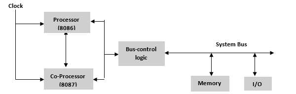
How is the coprocessor and the processor connected?
The coprocessor and the processor is connected via TEST, RQ-/GT- and QS0 & QS1 signals.
The TEST signal is connected to BUSY pin of coprocessor and the remaining 3 pins are connected to the coprocessor’s 3 pins of the same name.
TEST signal takes care of the coprocessor’s activity, i.e. the coprocessor is busy or idle.
The RT-/GT-is used for bus arbitration.
The coprocessor uses QS0 & QS1 to track the status of the queue of the host processor.
Closely Coupled Configuration
Closely coupled configuration is similar to the coprocessor configuration, i.e. both share the same memory, I/O system bus, control logic, and control generator with the host processor. However, the coprocessor and the host processor fetches and executes their own instructions. The system bus is controlled by the coprocessor and the host processor independently.
Block Diagram of Closely Coupled Configuration
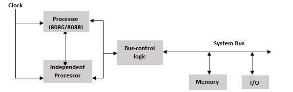
How is the processor and the independent processor connected?
Communication between the host and the independent processor is done through memory space.
None of the instructions are used for communication, like WAIT, ESC, etc.
The host processor manages the memory and wakes up the independent processor by sending commands to one of its ports.
Then the independent processor accesses the memory to execute the task.
After completion of the task, it sends an acknowledgement to the host processor by using the status signal or an interrupt request.
Loosely Coupled Configuration
Loosely coupled configuration consists of the number of modules of the microprocessor based systems, which are connected through a common system bus. Each module consists of their own clock generator, memory, I/O devices and are connected through a local bus.
Block Diagram of Loosely Coupled Configuration
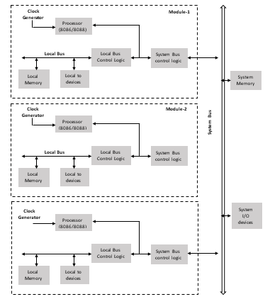
Advantages
Having more than one processor results in increased efficiency.
Each of the processors have their own local bus to access the local memory/I/O devices. This makes it easy to achieve parallel processing.
The system structure is flexible, i.e. the failure of one module doesn’t affect the whole system failure; faulty module can be replaced later.
8087 Numeric Data Processor
8087 numeric data processor is also known as Math co-processor, Numeric processor extension and Floating point unit. It was the first math coprocessor designed by Intel to pair with 8086/8088 resulting in easier and faster calculation.
Once the instructions are identified by the 8086/8088 processor, then it is allotted to the 8087 co-processor for further execution.
The data types supported by 8087 are −
- Binary Integers
- Packed decimal numbers
- Real numbers
- Temporary real format
The most prominent features of 8087 numeric data processor are as follows −
It supports data of type integer, float, and real types ranging from 2-10 bytes.
The processing speed is so high that it can calculate multiplication of two 64-bits real numbers in ~27 µs and can also calculate square-root in ~35 µs.
It follows IEEE floating point standards.
8087 Architecture
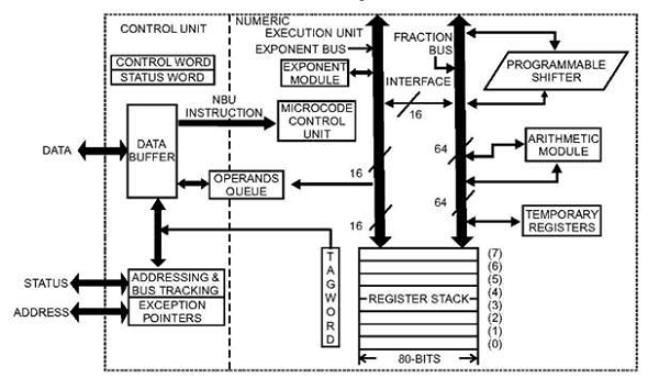
8087 Architecture is divided into two groups, i.e., Control Unit (CU) and Numeric Extension Unit (NEU).
The control unit handles all the communication between the processor and the memory such as it receives and decodes instructions, reads and writes memory operands, maintains parallel queue, etc. All the coprocessor instructions are ESC instructions, i.e., they start with ‘F’, the coprocessor only executes the ESC instructions while other instructions are executed by the microprocessor.
The numeric extension unit handles all the numeric processor instructions like arithmetic, logical, transcendental, and data transfer instructions. It has 8 register stack, which holds the operands for instructions and their results.
The architecture of 8087 coprocessor is as follows −
8087 Pin Description
Let us first take a look at the pin diagram of 8087 −
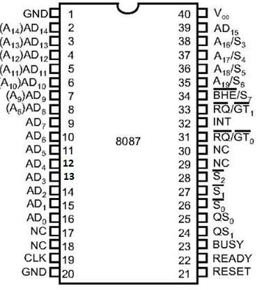
The following list provides the Pin Description of 8087 −
AD0 – AD15 − These are the time multiplexed address/data lines, which carry addresses during the first clock cycle and data from the second clock cycle onwards.
A19 / S6 – A16/S − These lines are the time multiplexed address/status lines. It functions in a similar way to the corresponding pins of 8086. The S6, S4 and S3 are permanently high, while the S5 is permanently low.
$\overline{BHE}$/S7 − During the first clock cycle, the $\overline{BHE}$/S7 is used to enable data on to the higher byte of the 8086 data bus and after that works as status line S7.
QS1, QS0 − These are queue status input signals which provides the status of instruction queue, their conditions as shown in the following table −
| QS0 | QS1 | Status |
|---|---|---|
| 0 | 0 | No operation |
| 0 | 1 | First byte of opcode from the queue |
| 1 | 0 | Empty the queue |
| 1 | 1 | Subsequent byte from the queue |
INT − It is an interrupt signal, which changes to high when an unmasked exception has been received during the execution.
BUSY − It is an output signal, when it is high it indicates a busy state to the CPU.
READY − It is an input signal used to inform the coprocessor whether the bus is ready to receive data or not.
RESET − It is an input signal used to reject the internal activities of the coprocessor and prepare it for further execution whenever required by the CPU.
CLK − The CLK input provides the basic timings for the processor operation.
VCC − It is a power supply signal, which requires +5V supply for the operation of the circuit.
S0, S1, S2 − These are the status signals that provide the status of the operation which is used by the Bus Controller 8087 to generate memory and I/O control signals. These signals are active during the fourth clock cycle.
| S2 | S1 | S0 | Queue Status |
|---|---|---|---|
| 0 | X | X | Unused |
| 1 | 0 | 0 | Unused |
| 1 | 0 | 1 | Memory read |
| 1 | 1 | 0 | Memory write |
| 1 | 1 | 1 | Passive |
RQ/GT1 & RQ/GT0 − These are the Request/Grant signals used by the 8087 processors to gain control of the bus from the host processor 8086/8088 for operand transfers.
Microprocessor - I/O Interfacing Overview
In this chapter, we will discuss Memory Interfacing and IO Interfacing with 8085.
Interface is the path for communication between two components. Interfacing is of two types, memory interfacing and I/O interfacing.
Memory Interfacing
When we are executing any instruction, we need the microprocessor to access the memory for reading instruction codes and the data stored in the memory. For this, both the memory and the microprocessor requires some signals to read from and write to registers.
The interfacing process includes some key factors to match with the memory requirements and microprocessor signals. The interfacing circuit therefore should be designed in such a way that it matches the memory signal requirements with the signals of the microprocessor.
IO Interfacing
There are various communication devices like the keyboard, mouse, printer, etc. So, we need to interface the keyboard and other devices with the microprocessor by using latches and buffers. This type of interfacing is known as I/O interfacing.
Block Diagram of Memory and I/O Interfacing
8085 Interfacing Pins
Following is the list of 8085 pins used for interfacing with other devices −
- A15 - A8 (Higher Address Bus)
- AD7 - AD0(Lower Address/Data Bus)
- ALE
- RD
- WR
- READY
Ways of Communication − Microprocessor with the Outside World?
There are two ways of communication in which the microprocessor can connect with the outside world.
- Serial Communication Interface
- Parallel Communication interface
Serial Communication Interface − In this type of communication, the interface gets a single byte of data from the microprocessor and sends it bit by bit to the other system serially and vice-a-versa.
Parallel Communication Interface − In this type of communication, the interface gets a byte of data from the microprocessor and sends it bit by bit to the other systems in simultaneous (or) parallel fashion and vice-a-versa.
8279 - Programmable Keyboard
8279 programmable keyboard/display controller is designed by Intel that interfaces a keyboard with the CPU. The keyboard first scans the keyboard and identifies if any key has been pressed. It then sends their relative response of the pressed key to the CPU and vice-a-versa.
How Many Ways the Keyboard is Interfaced with the CPU?
The Keyboard can be interfaced either in the interrupt or the polled mode. In the Interrupt mode, the processor is requested service only if any key is pressed, otherwise the CPU will continue with its main task.
In the Polled mode, the CPU periodically reads an internal flag of 8279 to check whether any key is pressed or not with key pressure.
How Does 8279 Keyboard Work?
The keyboard consists of maximum 64 keys, which are interfaced with the CPU by using the key-codes. These key-codes are de-bounced and stored in an 8-byte FIFORAM, which can be accessed by the CPU. If more than 8 characters are entered in the FIFO, then it means more than eight keys are pressed at a time. This is when the overrun status is set.
If a FIFO contains a valid key entry, then the CPU is interrupted in an interrupt mode else the CPU checks the status in polling to read the entry. Once the CPU reads a key entry, then FIFO is updated, and the key entry is pushed out of the FIFO to generate space for new entries.
Architecture and Description
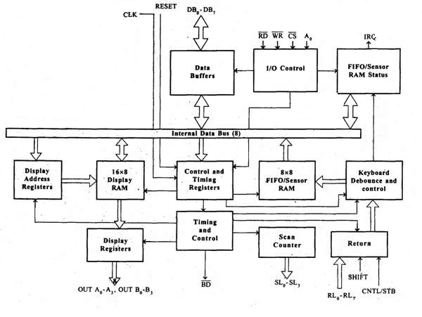
I/O Control and Data Buffer
This unit controls the flow of data through the microprocessor. It is enabled only when D is low. Its data buffer interfaces the external bus of the system with the internal bus of the microprocessor. The pins A0, RD, and WR are used for command, status or data read/write operations.
Control and Timing Register and Timing Control
This unit contains registers to store the keyboard, display modes, and other operations as programmed by the CPU. The timing and control unit handles the timings for the operation of the circuit.
Scan Counter
It has two modes i.e. Encoded mode and Decoded mode. In the encoded mode, the counter provides the binary count that is to be externally decoded to provide the scan lines for the keyboard and display.
In the decoded scan mode, the counter internally decodes the least significant 2 bits and provides a decoded 1 out of 4 scan on SL0-SL3.
Return Buffers, Keyboard Debounce, and Control
This unit first scans the key closure row-wise, if found then the keyboard debounce unit debounces the key entry. In case, the same key is detected, then the code of that key is directly transferred to the sensor RAM along with SHIFT & CONTROL key status.
FIFO/Sensor RAM and Status Logic
This unit acts as 8-byte first-in-first-out (FIFO) RAM where the key code of every pressed key is entered into the RAM as per their sequence. The status logic generates an interrupt request after each FIFO read operation till the FIFO gets empty.
In the scanned sensor matrix mode, this unit acts as sensor RAM where its each row is loaded with the status of their corresponding row of sensors into the matrix. When the sensor changes its state, the IRQ line changes to high and interrupts the CPU.
Display Address Registers and Display RAM
This unit consists of display address registers which holds the addresses of the word currently read/written by the CPU to/from the display RAM.
8279 − Pin Description
The following figure shows the pin diagram of 8279 −
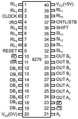
Data Bus Lines, DB0 - DB7
These are 8 bidirectional data bus lines used to transfer the data to/from the CPU.
CLK
The clock input is used to generate internal timings required by the microprocessor.
RESET
As the name suggests this pin is used to reset the microprocessor.
CS Chip Select
When this pin is set to low, it allows read/write operations, else this pin should be set to high.
A0
This pin indicates the transfer of command/status information. When it is low, it indicates the transfer of data.
RD, WR
This Read/Write pin enables the data buffer to send/receive data over the data bus.
IRQ
This interrupt output line goes high when there is data in the FIFO sensor RAM. The interrupt line goes low with each FIFO RAM read operation. However, if the FIFO RAM further contains any key-code entry to be read by the CPU, this pin again goes high to generate an interrupt to the CPU.
Vss, Vcc
These are the ground and power supply lines of the microprocessor.
SL0 − SL3
These are the scan lines used to scan the keyboard matrix and display the digits. These lines can be programmed as encoded or decoded, using the mode control register.
RL0 − RL7
These are the Return Lines which are connected to one terminal of keys, while the other terminal of the keys is connected to the decoded scan lines. These lines are set to 0 when any key is pressed.
SHIFT
The Shift input line status is stored along with every key code in FIFO in the scanned keyboard mode. Till it is pulled low with a key closure, it is pulled up internally to keep it high
CNTL/STB - CONTROL/STROBED I/P Mode
In the keyboard mode, this line is used as a control input and stored in FIFO on a key closure. The line is a strobe line that enters the data into FIFO RAM, in the strobed input mode. It has an internal pull up. The line is pulled down with a key closure.
BD
It stands for blank display. It is used to blank the display during digit switching.
OUTA0 – OUTA3 and OUTB0 – OUTB3
These are the output ports for two 16x4 or one 16x8 internal display refresh registers. The data from these lines is synchronized with the scan lines to scan the display and the keyboard.
Operational Modes of 8279
There are two modes of operation on 8279 − Input Mode and Output Mode.
Input Mode
This mode deals with the input given by the keyboard and this mode is further classified into 3 modes.
Scanned Keyboard Mode − In this mode, the key matrix can be interfaced using either encoded or decoded scans. In the encoded scan, an 8×8 keyboard or in the decoded scan, a 4×8 keyboard can be interfaced. The code of key pressed with SHIFT and CONTROL status is stored into the FIFO RAM.
Scanned Sensor Matrix − In this mode, a sensor array can be interfaced with the processor using either encoder or decoder scans. In the encoder scan, 8×8 sensor matrix or with decoder scan 4×8 sensor matrix can be interfaced.
Strobed Input − In this mode, when the control line is set to 0, the data on the return lines is stored in the FIFO byte by byte.
Output Mode
This mode deals with display-related operations. This mode is further classified into two output modes.
Display Scan − This mode allows 8/16 character multiplexed displays to be organized as dual 4-bit/single 8-bit display units.
Display Entry − This mode allows the data to be entered for display either from the right side/left side.
Microprocessor - 8257 DMA Controller
DMA stands for Direct Memory Access. It is designed by Intel to transfer data at the fastest rate. It allows the device to transfer the data directly to/from memory without any interference of the CPU.
Using a DMA controller, the device requests the CPU to hold its data, address and control bus, so the device is free to transfer data directly to/from the memory. The DMA data transfer is initiated only after receiving HLDA signal from the CPU.
How DMA Operations are Performed?
Following is the sequence of operations performed by a DMA −
Initially, when any device has to send data between the device and the memory, the device has to send DMA request (DRQ) to DMA controller.
The DMA controller sends Hold request (HRQ) to the CPU and waits for the CPU to assert the HLDA.
Then the microprocessor tri-states all the data bus, address bus, and control bus. The CPU leaves the control over bus and acknowledges the HOLD request through HLDA signal.
Now the CPU is in HOLD state and the DMA controller has to manage the operations over buses between the CPU, memory, and I/O devices.
Features of 8257
Here is a list of some of the prominent features of 8257 −
It has four channels which can be used over four I/O devices.
Each channel has 16-bit address and 14-bit counter.
Each channel can transfer data up to 64kb.
Each channel can be programmed independently.
Each channel can perform read transfer, write transfer and verify transfer operations.
It generates MARK signal to the peripheral device that 128 bytes have been transferred.
It requires a single phase clock.
Its frequency ranges from 250Hz to 3MHz.
It operates in 2 modes, i.e., Master mode and Slave mode.
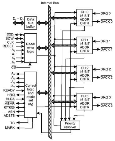
8257 Architecture
The following image shows the architecture of 8257 −
8257 Pin Description
The following image shows the pin diagram of a 8257 DMA controller −
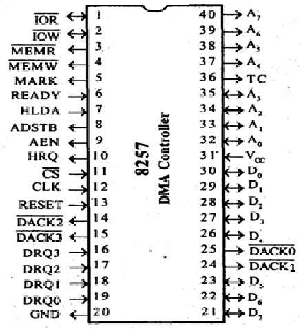
DRQ0−DRQ3
These are the four individual channel DMA request inputs, which are used by the peripheral devices for using DMA services. When the fixed priority mode is selected, then DRQ0 has the highest priority and DRQ3 has the lowest priority among them.
DACKo − DACK3
These are the active-low DMA acknowledge lines, which updates the requesting peripheral about the status of their request by the CPU. These lines can also act as strobe lines for the requesting devices.
Do − D7
These are bidirectional, data lines which are used to interface the system bus with the internal data bus of DMA controller. In the Slave mode, it carries command words to 8257 and status word from 8257. In the master mode, these lines are used to send higher byte of the generated address to the latch. This address is further latched using ADSTB signal.
IOR
It is an active-low bidirectional tri-state input line, which is used by the CPU to read internal registers of 8257 in the Slave mode. In the master mode, it is used to read data from the peripheral devices during a memory write cycle.
IOW
It is an active low bi-direction tri-state line, which is used to load the contents of the data bus to the 8-bit mode register or upper/lower byte of a 16-bit DMA address register or terminal count register. In the master mode, it is used to load the data to the peripheral devices during DMA memory read cycle.
CLK
It is a clock frequency signal which is required for the internal operation of 8257.
RESET
This signal is used to RESET the DMA controller by disabling all the DMA channels.
Ao - A3
These are the four least significant address lines. In the slave mode, they act as an input, which selects one of the registers to be read or written. In the master mode, they are the four least significant memory address output lines generated by 8257.
CS
It is an active-low chip select line. In the Slave mode, it enables the read/write operations to/from 8257. In the master mode, it disables the read/write operations to/from 8257.
A4 - A7
These are the higher nibble of the lower byte address generated by DMA in the master mode.
READY
It is an active-high asynchronous input signal, which makes DMA ready by inserting wait states.
HRQ
This signal is used to receive the hold request signal from the output device. In the slave mode, it is connected with a DRQ input line 8257. In Master mode, it is connected with HOLD input of the CPU.
HLDA
It is the hold acknowledgement signal which indicates the DMA controller that the bus has been granted to the requesting peripheral by the CPU when it is set to 1.
MEMR
It is the low memory read signal, which is used to read the data from the addressed memory locations during DMA read cycles.
MEMW
It is the active-low three state signal which is used to write the data to the addressed memory location during DMA write operation.
ADST
This signal is used to convert the higher byte of the memory address generated by the DMA controller into the latches.
AEN
This signal is used to disable the address bus/data bus.
TC
It stands for ‘Terminal Count’, which indicates the present DMA cycle to the present peripheral devices.
MARK
The mark will be activated after each 128 cycles or integral multiples of it from the beginning. It indicates the current DMA cycle is the 128th cycle since the previous MARK output to the selected peripheral device.
Vcc
It is the power signal which is required for the operation of the circuit.
Microcontrollers - Overview
A microcontroller is a small and low-cost microcomputer, which is designed to perform the specific tasks of embedded systems like displaying microwave’s information, receiving remote signals, etc.
The general microcontroller consists of the processor, the memory (RAM, ROM, EPROM), Serial ports, peripherals (timers, counters), etc.
Difference between Microprocessor and Microcontroller
The following table highlights the differences between a microprocessor and a microcontroller −
| Microcontroller | Microprocessor |
|---|---|
| Microcontrollers are used to execute a single task within an application. | Microprocessors are used for big applications. |
| Its designing and hardware cost is low. | Its designing and hardware cost is high. |
| Easy to replace. | Not so easy to replace. |
| It is built with CMOS technology, which requires less power to operate. | Its power consumption is high because it has to control the entire system. |
| It consists of CPU, RAM, ROM, I/O ports. | It doesn’t consist of RAM, ROM, I/O ports. It uses its pins to interface to peripheral devices. |
Types of Microcontrollers
Microcontrollers are divided into various categories based on memory, architecture, bits and instruction sets. Following is the list of their types −
Bit
Based on bit configuration, the microcontroller is further divided into three categories.
8-bit microcontroller − This type of microcontroller is used to execute arithmetic and logical operations like addition, subtraction, multiplication division, etc. For example, Intel 8031 and 8051 are 8 bits microcontroller.
16-bit microcontroller − This type of microcontroller is used to perform arithmetic and logical operations where higher accuracy and performance is required. For example, Intel 8096 is a 16-bit microcontroller.
32-bit microcontroller − This type of microcontroller is generally used in automatically controlled appliances like automatic operational machines, medical appliances, etc.
Memory
Based on the memory configuration, the microcontroller is further divided into two categories.
External memory microcontroller − This type of microcontroller is designed in such a way that they do not have a program memory on the chip. Hence, it is named as external memory microcontroller. For example: Intel 8031 microcontroller.
Embedded memory microcontroller − This type of microcontroller is designed in such a way that the microcontroller has all programs and data memory, counters and timers, interrupts, I/O ports are embedded on the chip. For example: Intel 8051 microcontroller.
Instruction Set
Based on the instruction set configuration, the microcontroller is further divided into two categories.
CISC − CISC stands for complex instruction set computer. It allows the user to insert a single instruction as an alternative to many simple instructions.
RISC − RISC stands for Reduced Instruction Set Computers. It reduces the operational time by shortening the clock cycle per instruction.
Applications of Microcontrollers
Microcontrollers are widely used in various different devices such as −
Light sensing and controlling devices like LED.
Temperature sensing and controlling devices like microwave oven, chimneys.
Fire detection and safety devices like Fire alarm.
Measuring devices like Volt Meter.
Microcontrollers - 8051 Architecture
8051 microcontroller is designed by Intel in 1981. It is an 8-bit microcontroller. It is built with 40 pins DIP (dual inline package), 4kb of ROM storage and 128 bytes of RAM storage, 2 16-bit timers. It consists of are four parallel 8-bit ports, which are programmable as well as addressable as per the requirement. An on-chip crystal oscillator is integrated in the microcontroller having crystal frequency of 12 MHz.
Let us now discuss the architecture of 8051 Microcontroller.
In the following diagram, the system bus connects all the support devices to the CPU. The system bus consists of an 8-bit data bus, a 16-bit address bus and bus control signals. All other devices like program memory, ports, data memory, serial interface, interrupt control, timers, and the CPU are all interfaced together through the system bus.
Microcontrollers - 8051 Pin Description
The pin diagram of 8051 microcontroller looks as follows −
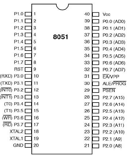
Pins 1 to 8 − These pins are known as Port 1. This port doesn’t serve any other functions. It is internally pulled up, bi-directional I/O port.
Pin 9 − It is a RESET pin, which is used to reset the microcontroller to its initial values.
Pins 10 to 17 − These pins are known as Port 3. This port serves some functions like interrupts, timer input, control signals, serial communication signals RxD and TxD, etc.
Pins 18 & 19 − These pins are used for interfacing an external crystal to get the system clock.
Pin 20 − This pin provides the power supply to the circuit.
Pins 21 to 28 − These pins are known as Port 2. It serves as I/O port. Higher order address bus signals are also multiplexed using this port.
Pin 29 − This is PSEN pin which stands for Program Store Enable. It is used to read a signal from the external program memory.
Pin 30 − This is EA pin which stands for External Access input. It is used to enable/disable the external memory interfacing.
Pin 31 − This is ALE pin which stands for Address Latch Enable. It is used to demultiplex the address-data signal of port.
Pins 32 to 39 − These pins are known as Port 0. It serves as I/O port. Lower order address and data bus signals are multiplexed using this port.
Pin 40 − This pin is used to provide power supply to the circuit.
Microcontrollers 8051 Input Output Ports
8051 microcontrollers have 4 I/O ports each of 8-bit, which can be configured as input or output. Hence, total 32 input/output pins allow the microcontroller to be connected with the peripheral devices.
Pin configuration, i.e. the pin can be configured as 1 for input and 0 for output as per the logic state.
Input/Output (I/O) pin − All the circuits within the microcontroller must be connected to one of its pins except P0 port because it does not have pull-up resistors built-in.
Input pin − Logic 1 is applied to a bit of the P register. The output FE transistor is turned off and the other pin remains connected to the power supply voltage over a pull-up resistor of high resistance.
Port 0 − The P0 (zero) port is characterized by two functions −
When the external memory is used then the lower address byte (addresses A0A7) is applied on it, else all bits of this port are configured as input/output.
When P0 port is configured as an output then other ports consisting of pins with built-in pull-up resistor connected by its end to 5V power supply, the pins of this port have this resistor left out.
Input Configuration
If any pin of this port is configured as an input, then it acts as if it “floats”, i.e. the input has unlimited input resistance and in-determined potential.
Output Configuration
When the pin is configured as an output, then it acts as an “open drain”. By applying logic 0 to a port bit, the appropriate pin will be connected to ground (0V), and applying logic 1, the external output will keep on “floating”.
In order to apply logic 1 (5V) on this output pin, it is necessary to build an external pullup resistor.
Port 1
P1 is a true I/O port as it doesn’t have any alternative functions as in P0, but this port can be configured as general I/O only. It has a built-in pull-up resistor and is completely compatible with TTL circuits.
Port 2
P2 is similar to P0 when the external memory is used. Pins of this port occupy addresses intended for the external memory chip. This port can be used for higher address byte with addresses A8-A15. When no memory is added then this port can be used as a general input/output port similar to Port 1.
Port 3
In this port, functions are similar to other ports except that the logic 1 must be applied to appropriate bit of the P3 register.
Pins Current Limitations
When pins are configured as an output (i.e. logic 0), then the single port pins can receive a current of 10mA.
When these pins are configured as inputs (i.e. logic 1), then built-in pull-up resistors provide very weak current, but can activate up to 4 TTL inputs of LS series.
If all 8 bits of a port are active, then the total current must be limited to 15mA (port P0: 26mA).
If all ports (32 bits) are active, then the total maximum current must be limited to 71mA.
Microcontrollers - 8051 Interrupts
Interrupts are the events that temporarily suspend the main program, pass the control to the external sources and execute their task. It then passes the control to the main program where it had left off.
8051 has 5 interrupt signals, i.e. INT0, TFO, INT1, TF1, RI/TI. Each interrupt can be enabled or disabled by setting bits of the IE register and the whole interrupt system can be disabled by clearing the EA bit of the same register.
IE (Interrupt Enable) Register
This register is responsible for enabling and disabling the interrupt. EA register is set to one for enabling interrupts and set to 0 for disabling the interrupts. Its bit sequence and their meanings are shown in the following figure.

| EA | IE.7 | It disables all interrupts. When EA = 0 no interrupt will be acknowledged and EA = 1 enables the interrupt individually. |
| - | IE.6 | Reserved for future use. |
| - | IE.5 | Reserved for future use. |
| ES | IE.4 | Enables/disables serial port interrupt. |
| ET1 | IE.3 | Enables/disables timer1 overflow interrupt. |
| EX1 | IE.2 | Enables/disables external interrupt1. |
| ET0 | IE.1 | Enables/disables timer0 overflow interrupt. |
| EX0 | IE.0 | Enables/disables external interrupt0. |
IP (Interrupt Priority) Register
We can change the priority levels of the interrupts by changing the corresponding bit in the Interrupt Priority (IP) register as shown in the following figure.
A low priority interrupt can only be interrupted by the high priority interrupt, but not interrupted by another low priority interrupt.
If two interrupts of different priority levels are received simultaneously, the request of higher priority level is served.
If the requests of the same priority levels are received simultaneously, then the internal polling sequence determines which request is to be serviced.

| - | IP.6 | Reserved for future use. |
| - | IP.5 | Reserved for future use. |
| PS | IP.4 | It defines the serial port interrupt priority level. |
| PT1 | IP.3 | It defines the timer interrupt of 1 priority. |
| PX1 | IP.2 | It defines the external interrupt priority level. |
| PT0 | IP.1 | It defines the timer0 interrupt priority level. |
| PX0 | IP.0 | It defines the external interrupt of 0 priority level. |
TCON Register
TCON register specifies the type of external interrupt to the microcontroller.
8255A - Programmable Peripheral Interface
The 8255A is a general purpose programmable I/O device designed to transfer the data from I/O to interrupt I/O under certain conditions as required. It can be used with almost any microprocessor.
It consists of three 8-bit bidirectional I/O ports (24I/O lines) which can be configured as per the requirement.
Ports of 8255A
8255A has three ports, i.e., PORT A, PORT B, and PORT C.
Port A contains one 8-bit output latch/buffer and one 8-bit input buffer.
Port B is similar to PORT A.
Port C can be split into two parts, i.e. PORT C lower (PC0-PC3) and PORT C upper (PC7-PC4) by the control word.
These three ports are further divided into two groups, i.e. Group A includes PORT A and upper PORT C. Group B includes PORT B and lower PORT C. These two groups can be programmed in three different modes, i.e. the first mode is named as mode 0, the second mode is named as Mode 1 and the third mode is named as Mode 2.
Operating Modes
8255A has three different operating modes −
Mode 0 − In this mode, Port A and B is used as two 8-bit ports and Port C as two 4-bit ports. Each port can be programmed in either input mode or output mode where outputs are latched and inputs are not latched. Ports do not have interrupt capability.
Mode 1 − In this mode, Port A and B is used as 8-bit I/O ports. They can be configured as either input or output ports. Each port uses three lines from port C as handshake signals. Inputs and outputs are latched.
Mode 2 − In this mode, Port A can be configured as the bidirectional port and Port B either in Mode 0 or Mode 1. Port A uses five signals from Port C as handshake signals for data transfer. The remaining three signals from Port C can be used either as simple I/O or as handshake for port B.
Features of 8255A
The prominent features of 8255A are as follows −
It consists of 3 8-bit IO ports i.e. PA, PB, and PC.
Address/data bus must be externally demux'd.
It is TTL compatible.
It has improved DC driving capability.
8255 Architecture
The following figure shows the architecture of 8255A −
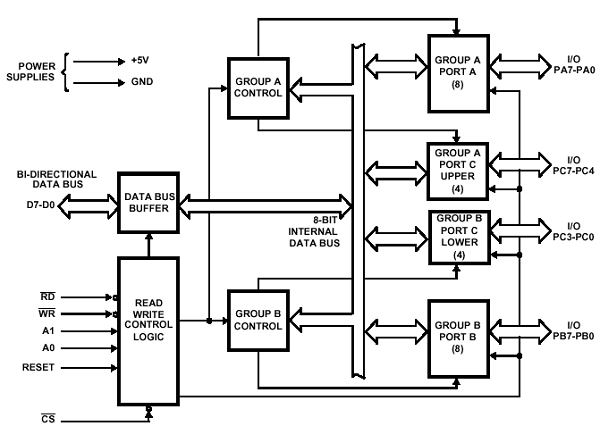
Intel 8255A - Pin Description
Let us first take a look at the pin diagram of Intel 8255A −
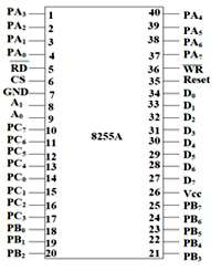
Now let us discuss the functional description of the pins in 8255A.
Data Bus Buffer
It is a tri-state 8-bit buffer, which is used to interface the microprocessor to the system data bus. Data is transmitted or received by the buffer as per the instructions by the CPU. Control words and status information is also transferred using this bus.
Read/Write Control Logic
This block is responsible for controlling the internal/external transfer of data/control/status word. It accepts the input from the CPU address and control buses, and in turn issues command to both the control groups.
CS
It stands for Chip Select. A LOW on this input selects the chip and enables the communication between the 8255A and the CPU. It is connected to the decoded address, and A0 & A1 are connected to the microprocessor address lines.
Their result depends on the following conditions −
| CS | A1 | A0 | Result |
|---|---|---|---|
| 0 | 0 | 0 | PORT A |
| 0 | 0 | 1 | PORT B |
| 0 | 1 | 0 | PORT C |
| 0 | 1 | 1 | Control Register |
| 1 | X | X | No Selection |
WR
It stands for write. This control signal enables the write operation. When this signal goes low, the microprocessor writes into a selected I/O port or control register.
RESET
This is an active high signal. It clears the control register and sets all ports in the input mode.
RD
It stands for Read. This control signal enables the Read operation. When the signal is low, the microprocessor reads the data from the selected I/O port of the 8255.
A0 and A1
These input signals work with RD, WR, and one of the control signal. Following is the table showing their various signals with their result.
| A1 | A0 | RD | WR | CS | Result |
|---|---|---|---|---|---|
| 0 | 0 | 0 | 1 | 0 | Input Operation PORT A → Data Bus |
| 0 | 1 | 0 | 1 | 0 | PORT B → Data Bus |
| 1 | 0 | 0 | 1 | 0 | PORT C → Data Bus |
| 0 | 0 | 1 | 0 | 0 | Output Operation Data Bus → PORT A |
| 0 | 1 | 1 | 0 | 0 | Data Bus → PORT A |
| 1 | 0 | 1 | 0 | 0 | Data Bus → PORT B |
| 1 | 1 | 1 | 0 | 0 | Data Bus → PORT D |
Intel 8253 - Programmable Interval Timer
The Intel 8253 and 8254 are Programmable Interval Timers (PTIs) designed for microprocessors to perform timing and counting functions using three 16-bit registers. Each counter has 2 input pins, i.e. Clock & Gate, and 1 pin for “OUT” output. To operate a counter, a 16-bit count is loaded in its register. On command, it begins to decrement the count until it reaches 0, then it generates a pulse that can be used to interrupt the CPU.
Difference between 8253 and 8254
The following table differentiates the features of 8253 and 8254 −
| 8253 | 8254 |
|---|---|
| Its operating frequency is 0 - 2.6 MHz | Its operating frequency is 0 - 10 MHz |
| It uses N-MOS technology | It uses H-MOS technology |
| Read-Back command is not available | Read-Back command is available |
| Reads and writes of the same counter cannot be interleaved. | Reads and writes of the same counter can be interleaved. |
Features of 8253 / 54
The most prominent features of 8253/54 are as follows −
It has three independent 16-bit down counters.
It can handle inputs from DC to 10 MHz.
These three counters can be programmed for either binary or BCD count.
It is compatible with almost all microprocessors.
8254 has a powerful command called READ BACK command, which allows the user to check the count value, the programmed mode, the current mode, and the current status of the counter.
8254 Architecture
The architecture of 8254 looks as follows −
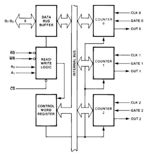
8254 Pin Description
Here is the pin diagram of 8254 −
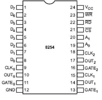
In the above figure, there are three counters, a data bus buffer, Read/Write control logic, and a control register. Each counter has two input signals - CLOCK & GATE, and one output signal - OUT.
Data Bus Buffer
It is a tri-state, bi-directional, 8-bit buffer, which is used to interface the 8253/54 to the system data bus. It has three basic functions −
- Programming the modes of 8253/54.
- Loading the count registers.
- Reading the count values.
Read/Write Logic
It includes 5 signals, i.e. RD, WR, CS, and the address lines A0 & A1. In the peripheral I/O mode, the RD and WR signals are connected to IOR and IOW, respectively. In the memorymapped I/O mode, these are connected to MEMR and MEMW.
Address lines A0 & A1 of the CPU are connected to lines A0 and A1 of the 8253/54, and CS is tied to a decoded address. The control word register and counters are selected according to the signals on lines A0 & A1.
| A1 | A0 | Result |
|---|---|---|
| 0 | 0 | Counter 0 |
| 0 | 1 | Counter 1 |
| 1 | 0 | Counter 2 |
| 1 | 1 | Control Word Register |
| X | X | No Selection |
Control Word Register
This register is accessed when lines A0 & A1 are at logic 1. It is used to write a command word, which specifies the counter to be used, its mode, and either a read or write operation. Following table shows the result for various control inputs.
| A1 | A0 | RD | WR | CS | Result |
|---|---|---|---|---|---|
| 0 | 0 | 1 | 0 | 0 | Write Counter 0 |
| 0 | 1 | 1 | 0 | 0 | Write Counter 1 |
| 1 | 0 | 1 | 0 | 0 | Write Counter 2 |
| 1 | 1 | 1 | 0 | 0 | Write Control Word |
| 0 | 0 | 0 | 1 | 0 | Read Counter 0 |
| 0 | 1 | 0 | 1 | 0 | Read Counter 1 |
| 1 | 0 | 0 | 1 | 0 | Read Counter 2 |
| 1 | 1 | 0 | 1 | 0 | No operation |
| X | X | 1 | 1 | 0 | No operation |
| X | X | X | X | 1 | No operation |
Counters
Each counter consists of a single, 16 bit-down counter, which can be operated in either binary or BCD. Its input and output is configured by the selection of modes stored in the control word register. The programmer can read the contents of any of the three counters without disturbing the actual count in process.
Intel 8253/54 - Operational Modes
8253/54 can be operated in 6 different modes. In this chapter, we will discuss these operational modes.
Mode 0 ─ Interrupt on Terminal Count
It is used to generate an interrupt to the microprocessor after a certain interval.
Initially the output is low after the mode is set. The output remains LOW after the count value is loaded into the counter.
The process of decrementing the counter continues till the terminal count is reached, i.e., the count become zero and the output goes HIGH and will remain high until it reloads a new count.
The GATE signal is high for normal counting. When GATE goes low, counting is terminated and the current count is latched till the GATE goes high again.
Mode 1 – Programmable One Shot
It can be used as a mono stable multi-vibrator.
The gate input is used as a trigger input in this mode.
The output remains high until the count is loaded and a trigger is applied.
Mode 2 – Rate Generator
The output is normally high after initialization.
Whenever the count becomes zero, another low pulse is generated at the output and the counter will be reloaded.
Mode 3 – Square Wave Generator
This mode is similar to Mode 2 except the output remains low for half of the timer period and high for the other half of the period.
Mode 4 − Software Triggered Mode
In this mode, the output will remain high until the timer has counted to zero, at which point the output will pulse low and then go high again.
The count is latched when the GATE signal goes LOW.
On the terminal count, the output goes low for one clock cycle then goes HIGH. This low pulse can be used as a strobe.
Mode 5 – Hardware Triggered Mode
This mode generates a strobe in response to an externally generated signal.
This mode is similar to mode 4 except that the counting is initiated by a signal at the gate input, which means it is hardware triggered instead of software triggered.
After it is initialized, the output goes high.
When the terminal count is reached, the output goes low for one clock cycle.